TOTAL REACH NETWORK microNode Integration Specification On-Ramp Wireless Confidential and Proprietary. This document is not to be used, disclosed, or distributed to anyone without express written consent from On-Ramp Wireless, Inc. The recipient of this document shall respect the security of this document and maintain the confidentiality of the information it contains.
On-Ramp Wireless, Inc. 10920 Via Frontera, Suite 200 San Diego, CA 92127 U.S.A. Copyright © 2015 On-Ramp Wireless, Inc. All Rights Reserved. The information disclosed in this document is proprietary to On-Ramp Wireless, Inc. and is not to be used or disclosed to unauthorized persons without the written consent of On-Ramp Wireless, Inc. The recipient of this document shall respect the security of this document and maintain the confidentiality of the information it contains.
Contents 1 Overview ................................................................................................................ 1 1.1 On-Ramp Total Reach Wireless Network .................................................................................. 1 1.2 microNode .................................................................................................................................. 2 1.3 Referenced Documents ..............................................................................
microNode Integration Specification Contents 4.5.1 Wake Sequence (Synchronous) ..................................................................................... 19 4.5.2 Wake Sequence (Asynchronous) ................................................................................... 20 4.6 Host-Driven Reset Sequence .................................................................................................. 21 4.7 Host MRQ Release/microNode Allowed to Sleep Sequence ..............................
microNode Integration Specification Contents 10 Manufacturing Considerations ........................................................................ 47 10.1 Mechanical Outline................................................................................................................. 47 10.2 Host PCB Constraints ............................................................................................................ 47 10.3 Handling Procedures for microNode ........................................
microNode Integration Specification Contents Figure 20. Host Message on SPI – MHdr Pair ............................................................................... 33 Figure 21. Antenna Diversity Circuit .............................................................................................. 38 Figure 22. microNode Block Diagram ............................................................................................ 41 Figure 23. Product Label ................................................
Revision History Revision Release Date Change Description A January 18, 2012 Initial release. B March 13, 2012 C May 24, 2012 D July 11, 2012 E September 14, 2012 Added more detail about the microNode in the Overview chapter. Updated notes below the Operating Characteristics table relating to transmit power configuration during provisioning. F May 13, 2014 Expanded information for regulatory considerations and certifications. Removed errata section that is no longer relevant.
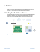
1 Overview This document provides a brief overview of the On-Ramp Total Reach wireless network as well as guidelines allowing an integrator to design a Host product that utilizes the microNode and ensures that the system meets all of its technical objectives and requirements. 1.1 On-Ramp Total Reach Wireless Network The On-Ramp Total Reach wireless network is comprised of microNodes and Access Points (AP).
microNode Integration Specification Overview 1.2 microNode The microNode is a small form factor wireless network module that easily integrates with various devices and sensors using an industry standard Serial Peripheral Interface (SPI). There are two versions of the microNode. The primary difference between the two versions of the microNode is transmit power. The following table summarizes the differences and recommendations. Table 1.
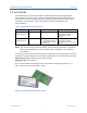
microNode Integration Specification Overview The following figure shows how a microNode interfaces with a Host application. Figure 3. Typical Application Diagram 1.3 Referenced Documents The following documents are referenced and provide more detail. EMC Compliance Guide (010-0037-00) Provides information for “driving” the Node through various modes in order to perform regulatory tests for FCC and ETSI.
2 DC and AC Characteristics 2.1 Absolute Maximum Ratings Operating outside of these ranges may damage the unit. The microNode is MSL 3-rated and should be handled as an MSL 3 device per IPC/JEDEC J-STD033 (latest revision). See section 10.3 for further information. Table 2. Absolute Maximum Ratings Parameter Min Max Unit Storage Temperature -40 85 ⁰C Operating Temperature -40 85 ⁰C Input Voltage 2.2 6.0 V 3.6 V 3 Digital Interface Signals, 3.3V nominal 2.
microNode Integration Specification DC and AC Characteristics Description Min Typ Max Units Environmental Operating Temperature -40 +85 °C Storage Temp -40 +85 °C Humidity – non-condensing 5 95 % 30 °C/Hr. Ramp Temperature (maximum rate at which operating temperature should change) MTBF (microNode1) 10.5 MHrs MTBF (microNode2) 6.4 MHrs Receiver Receiver Sensitivity – Note 3 -130 -133 -135 dBm Receiver Image Reject 38 45 50 dB Noise Figure 3.5 5.0 6.
microNode Integration Specification DC and AC Characteristics a. There are power differences between the Voltage/Current numbers in this table and the data provided in Figure 4, Figure 5, and Figure 6. These figures show representative characterization of Power over Voltage/Temperature characterization and are only representative behavior. 2. 3. 4. 5. 6. 7. 8. 9. 10. b. The Table 4 refers to a maximal current draw that the Host system should be designed to accommodate. Measured at: microNode1: +20.
microNode Integration Specification DC and AC Characteristics 1. LDO Regulators that work from 2.2V up to 5.5V. These are enabled when the POWER_ON signal for the microNode is active. These can act as a linear load as voltage increases from minimum to maximum – although these circuits do not normally consume much power. 2. Switching power domains. When the microNode wakes up to communicate with the Host or for networking events, its switching regulators are enabled.
microNode Integration Specification DC and AC Characteristics 380 -40C RX 370 -30C RX -20C RX 360 -10C RX 0C RX 350 10C RX 340 20C RX 330 30C RX 40C RX 320 50C RX 310 60C RX 300 70C RX 2 2.5 3 3.5 4 4.5 5 5.5 Figure 5. RX State Power Consumption (mW Power vs VBATT Input) 1030 -40C TX max -30C TX max 1010 -20C TX max -10C TX max 990 0C TX max 970 10C TX max 20C TX max 950 30C TX max 40C TX max 930 50C TX max 60C TX max 910 70C TX max 80C TX max 890 2 2.5 3 3.
microNode Integration Specification DC and AC Characteristics 1.1 1.05 1 0.95 -40C 0.9 -20C 0 0.85 +25C 0.8 +50C 0.75 +85C 0.7 0.65 0.6 1.5 2.5 3.5 4.5 5.5 6.5 Figure 7. microNode2: TX Power Consumption at 23.3 dBm (Watts Power vs VBATT Input) On-Ramp Wireless, Inc. 9 014-0033-00 Rev.
3 Electrical Interface This chapter describes the electrical interface of the microNode and how the Host processor controls the microNode. Table 5. microNode Pin Descriptions Pin # Pin Name Signal Direction Relative to microNode Signal Type Comment 1, 2, 3, 4, 7, 10 Ground Power Power Ground return. Should be low RF impedance to a solid ground plane of the Host 11,14, 17, 20, 21, 26, 30, 31, 34, 35, 37, 38, 40 Ground Power Power 5, 6 VBATT Power Power Input power to the microNode.
microNode Integration Specification Electrical Interface Pin # Pin Name Signal Direction Relative to microNode Signal Type Comment 28 UART_SOUT Output CMOS_O UART Serial output. Not supported at this time. 29 TOUT Output CMOS_O TOUT is a normally low signal that pulses high in response to specific Network Timing Events 32 RF_PAEN_EXT Input CMOS_I This is used to force the PA off. It is internally pulled low. Do not connect at this time.
microNode Integration Specification Electrical Interface 5. VBATT a. The microNode operating voltage is 2.2V - 5.5V, which drives a buck/boost regulator (3.3V) internal to the microNode. b. The internal 3.3V regulator drives the RF and PA circuitry of the microNode which also drives its operating CMOS I/O voltages. 6. CMOS_I The Node input voltages are 3.3V CMOS levels. VIH = 2.0V (minimum) and VIL = 0.8V (maximum). 7. CMOS_O The Node output voltages are 3.3V CMOS levels (4mA). VOH = 2.
microNode Integration Specification Electrical Interface 3.1.4 MRQ The MRQ (Master Request) is the Host’s normal way of waking the microNode to initiate SPI communications. Logic “High” forces the microNode awake. 3.1.5 SRDY SRDY (Slave Ready) is an indication from the microNode that it has fully booted its internal Firmware image, initialized its Hardware and Interfaces, and is ready for communication (arbitration) with the Host. Logic “High” indicates the microNode is ready for communications. 3.1.
microNode Integration Specification Electrical Interface 3.1.12 TOUT This signal is a Time Synchronizing signal that pulses high upon specific network timing events. 3.1.13 RF_PAEN_EXT The RF_PAEN_EXT signal is a direct hardware signal that can be used to disable the Power Amplifier (PA) for the microNode. This signal is pulled low (100k to ground) to allow the PA to work as normal. A microNode external device can temporarily assert this signal high to de-key the PA for the microNode.
microNode Integration Specification Electrical Interface The RF port does have some protection in the form of an inductor to ground, thus allowing some robustness to direct ESD strikes. If the application is intended for harsh ESD or lightning strike scenarios it is recommended that the Integrator take extra precautions to guard against accidental resets or ESD damage. 3.2.2 Harsh Environments The microNode employs miniature surface-mounted components in its assembly.
4 SPI Interface and Sequences 4.1 SPI System Interface Overview The SPI slave interface is currently the only supported interface for Host-to-Node communication. NOTE: The microNode must be the only SPI slave on the bus. The SPI slave interface provides communication with an external Host through a 7-wire interface. The Host is the SPI master and the microNode is the SPI slave. In addition to the four standard SPI signals, three additional signals are used to complement the SPI bus: MRQ, SRQ, and SRDY.
microNode Integration Specification SPI Interface and Sequences 4.2 SPI Mode and Timing SPCK Cycle (for reference) 1 2 3 4 5 6 7 8 SPCK (CPOL = 0) MOSI (from master) MISO (from slave) MSB MSB 6 5 4 3 2 1 LSB 6 5 4 3 2 1 LSB * NSS (to slave) Figure 8. SPI Timing, CPOL = 0, CPHA = 0 4.3 Host Initialization What is described here is the initialization of the Host, its operating software, and the control sequences used to drive the microNode.
microNode Integration Specification SPI Interface and Sequences VBATT Host Init (not a signal) Power On Reset_N MRQ Hi-Z SPI System SRDY 100 ms t0 t1 10 ms 1000 ms t2 t3 4 ms t4 t5 t6 t6 – t4 < 300 ms or error Figure 9. microNode Power-up Timing Sequence The timing sequence shown in Figure 9 above is described below. NOTE: The timing shown in the figure is not to scale.
microNode Integration Specification SPI Interface and Sequences t5 After the assertion of t4, the microNode begins its “wake sequence.” The microNode must boot, initialize its operating system and hardware and when it is ready for communications it raises its SRDY signal back to the Host. At this point, communications (Arbitration) can begin. t6 At this point the microNode signals its readiness by asserting the SRDY pin. The Host can now begin communications with the microNode. 4.
microNode Integration Specification SPI Interface and Sequences The timing sequence shown in Figure 10 above is described below. NOTE: The timing shown in the figure is not to scale. t0 The Host desires to wake the microNode and asserts MRQ high. t0 t1 After MRQ has gone High, the Host’s SPI system and other I/O can be enabled. Asserting the MRQ has enabled the internal I/O power supply of the microNode and the Host’s SPI can be enabled 4 ms after the rise of MRQ.
microNode Integration Specification SPI Interface and Sequences 4.6 Host-Driven Reset Sequence If the microNode fails to communicate (or similar), it may be necessary to Reset the microNode. The following figure shows the proper sequence to reset the device. NOTE 1: Resetting the device causes it to go through a Cold Acquisition process to reacquire the network. NOTE 2: The timing shown in the figure is not to scale.
microNode Integration Specification SPI Interface and Sequences 4.7 Host MRQ Release/microNode Allowed to Sleep Sequence If the Host determines there are no more messages or SPI transactions required, it nominally deasserts the MRQ to allow the microNode to fall back to Deep Sleep (lowest power mode). The figure below shows how this is sequenced by the Host/microNode. A small delay in de-asserting SRDY is enforced to prevent quick toggling (waking) of the microNode.
5 Power States The microNode has a number of states it runs through during its various operating modes. General comments: 1. The microNode accepts a wide input voltage range (2.2-5.5V). 2. The microNode has low drop out (LDO) regulators that will operate 100% of the time the microNode is powered (POWER_ON signal set high). 3. There are 3.3V/1.2V Buck/Boost Switching regulators that use the wide input range to drive key RF and Digital circuits. The 3.
microNode Integration Specification Power States 5.1.2 Deep Sleep State The microNode shuts off all its power regulators except a couple low quiescent LDO regulators. These regulators keep a minimal amount of circuitry alive for tracking network timers, enable a 32 kHz clock, and some minor interface circuitry. 5.1.
microNode Integration Specification Power States 5.1.4 Idle State Idle state has various sub-states but generally refers to a state where the microNode is “awake” and its system clock is on, the CPU is awake, but the RF is OFF. 5.1.5 RX State The microNode turns on all its clocks, the main CPU and the RF in an RX-only state. The RF transceiver, in RX state, consumes a moderate amount of power. 5.1.
microNode Integration Specification Power States Figure 15. Representative Current Consumption During Deep Sleep, Idle, RX, and TX; x16 Spreading Factor (Amps vs Seconds) The plot shown in the figure above represents the nominal transitions for the microNode from Deep Sleep, Idle, Receive, and Transmit states. In this case, a TX spreading factor of 16 is used.
6 Messaging Protocol The details of Host/Node messaging are typically not necessary for integrators to implement; however, low-level understanding of the SPI protocol used may be critical in resolving Host interface issues. For mid-level details of the messages that may be sent over this interface, refer to Node Host Message Specification (014-0020-00). 6.1 Arbitration Arbitration is the process a Host uses to signal to the Node that it supports the On-Ramp Wireless bi-directional messaging protocol.
microNode Integration Specification Messaging Protocol After a successful message request transfer, the Host waits a turn-around delay and then initiates the transfer with a message header command. The payload immediately follows the header and, if necessary, is zero padded to match the payload size indicated in the message request. After the payload, the Host waits a turn-around delay before proceeding with any other further messages.
microNode Integration Specification Messaging Protocol Node Host Slave Request MRQ=1 Arbitration Slave Ready SRDY=1 Arbitration Acknowledge ArbREQ ArbACK Validation Acknowledge ValREQ ValACK wait Arbitration Request wait Validation Request MRQ=1 SRDY=1 wait Host-to- Node Message Transfer MMsgREQ+Size MMsgACK+Size Master Message Acknowledge Master Message Request wait Master Header Acknowledge MHdrREQ MHdrACK Payload Receive PAYLOAD Master Header Request Payload Transmit wait Repeat 5
microNode Integration Specification Messaging Protocol bubbles indicate a predefined turn-around delay which provides ISR processing time and avoids race conditions between Host and Node. 6.3 Host Interface SPI Bus State Machine This section illustrates the sequence of messages that can take place on the Host interface SPI bus. The design and implementation of the actual state machine on the Host software is up to the Host software designer.
microNode Integration Specification Messaging Protocol 6.4 SPI Bus Timing Example This section provides an example illustration of an exchange of messages first from master (Host) to slave (Node) and then from slave (Node) to master (Host). Each step in the timing sequence is described below: 9 SRQ MRQ SRDY 6 10 5 1 11 2 CS SCLK MISO MOSI 3 4 7 8 Figure 18. SPI Timing Example Note that MRQ state transitions must respect the timing requirements shown in Chapter 4.
microNode Integration Specification Messaging Protocol 6. At some time in the future, the Node desires to send a message to the Host. It indicates this to the Host by driving SRQ high. Since SRQ is high, the Host drives MRQ and then CS high. It then waits for SRDY to go high, which it already is. 7. The Host starts the SPI data transaction.
microNode Integration Specification Messaging Protocol MOSI) are read on the SCLK rising edge and are set or cleared on the SCLK falling edge, and is commonly referred to as CPOL=0, CPHA=0.
microNode Integration Specification Messaging Protocol opcode=MHdrACK (1010) Hard coded byte=1 (00000001) Unused Extra Data (0000…...0) MOSI: from master to slave (10) length of message=2 (10) opcode =MhdrREQ (1010) Hard coded byte=1 (00000001) Payload: length=8 (0000100000000000) message type=VERSION (0001010101000000) trailing sequence (11110000111100001010010110100101) The payload is Little Endian. The least significant byte is transmitted over SPI first.
microNode Integration Specification Messaging Protocol opcode =MmsgREQ (1001) payload size=6 (00000110) The MMsg exchange is followed by the MHdr exchange, which includes the payload of the CONNECT message.
microNode Integration Specification Messaging Protocol These bits indicate: MISO: from slave to master (01) length of message=2 (10) opcode=SMsgACK (1011) buffer size=255 (11111111) payload size=4 (00000100) MOSI: from master to slave (10) length of message=2 (10) opcode =SmsgREQ (1011) buffer size=255 (11111111) The SMsg exchange is followed by the SHdr exchange, which includes the payload of the ACK message.
7 microNode Provisioning Provisioning a node consists of updating (if necessary) node firmware version, applying a configuration to the node, and providing security keys to the node. The node configuration and security keys must match the target network where the node will be deployed and, after provisioning, the node-specific key must be provided to the network operator. The provisioning software package is used to perform these steps.
8 Antenna Diversity The microNode supports Antenna Diversity for optimal System performance. In many cases, the microNode and Host system are mounted in fixed locations that often experience nulls in the RF coverage. Antenna Diversity can help with optimization of the RX and TX paths.
microNode Integration Specification Antenna Diversity 8.1 Antenna Design Considerations Good antenna design is also crucial to success. It is important to consider some pertinent issues. Ceramic antennas can work well but may sometimes have issues. Careful testing must be done to ensure desired gains and radiation patterns. The product must be researched in conjunction to the Access Point, its deployment, and its antenna radiation pattern.
9 Regulatory Considerations The microNode uses a castellation for its RF port. This lowers the unit cost and provides greater host configuration flexibility in the final application. On-Ramp Wireless has obtained modular certifications (FCC, IC, ETSI, Japan and others) for the microNode. The existence of the modular certification minimizes cost and time to market for our customers. The certification documents and the results of the certification tests are available to system integrators upon request.
microNode Integration Specification Regulatory Considerations Figure 22. microNode Block Diagram 9.2 Antennas This microNode has been certified to operate with the antennas listed below. To adhere to these certifications requires the antennas to be of the types specified below and of lower gain. In all instances, the combinations of microNode maximum transmit power and antenna gain must not exceed the regulatory Effective Isotropic Radiated Power (EIRP).
microNode Integration Specification Regulatory Considerations Table 8. microNode2: On-Ramp Wireless EMC Certified Antenna Manufacturer Part Number Gain Type Connector Comment Alfa Network ARS-N19 9 dBi Monopole RP-SMA Plug MMCX Plug to RP-SMA Jack adaptor required. Customers are free to follow one of two paths in their final product: Customers can use one of On-Ramp Wireless’ approved antenna types shown above that are of equal and lesser gain.
microNode Integration Specification Regulatory Considerations B unintentional radiator and powerline conducted emissions tests. This should be done with the actual production antenna. ETSI Europe’s system is a self-declaration system. There are no documents to submit or certification grants to obtain. One must have the passing test results available for all applicable requirements at any time if challenged. Other countries will vary. 9.
microNode Integration Specification Regulatory Considerations Operation is subject to the following two conditions: 1. This device may not cause harmful interference. 2. This device must accept any interference received, including interference that may cause undesired operation. To reduce potential radio interference to other users, select the antenna type and its gain so that the equivalent isotropically radiated power (EIRP) is not more than that permitted for successful communication.
microNode Integration Specification Regulatory Considerations Figure 23. Product Label If the microNode is contained within a product and is not visible, a label showing the FCC ID and IC designators (listed above) must be affixed to the exterior of the device containing the microNode. The exterior label must state the following: Table 11.
microNode Integration Specification Regulatory Considerations 9.10 RoHS Directive The microNodes comply with RoHS directive 2002/95/EC. On-Ramp Wireless has received Certificates of Conformance (CoC) for all components, printed circuit boards, and contract manufacturers for the microNodes. The RoHS Certification of Conformance is provided in Appendix C. 9.
10 Manufacturing Considerations This section deals with manufacturing details such as: Design of Host PCB for mounting the microNode The manufacturing process and soldering profile The validation and configuration of the microNode after the assembly process. 10.1 Mechanical Outline The microNode is a bottom termination component (BTC) that is designed to be directly surfacemounted onto a Host PCB.
11 Errata Degraded RF Channels The microNode uses a Channel scheme such as the following: Channel 1 = 2402 MHz and each successive channel is 1.99 MHz offset to that Channel 1. Channel 2 = 2403.99 MHz Channel 3 = 2405.98 MHz Etc. The microNode uses a 26 MHz reference clock for processing and for the direct conversion radio. It has been found that 26 MHz harmonics can create strong tones that cause some RF sensitivity degradation on these harmonic channels. 93*26 MHz = 2418 MHz.
Appendix A Abbreviations and Terms Abbreviation/Term Definition AGC Automatic Gain Control ALC Automatic Level Control AP Access Point API Application Programming Interface ASIC Application-Specific Integrated Circuit BOM Bill of Materials BW Bandwidth CCATS Commodity Classification Automated Tracking System. An alphanumeric code assigned by the Bureau of Industry and Security (BIS) to products that it has classified against the Export Administration Regulations (EAR).
microNode Integration Specification Abbreviations and Terms Abbreviation/Term Definition Node The generic term used interchangeably with microNode. On-Ramp Total Reach The On-Ramp Wireless’ proprietary wireless communication technology and network.
Appendix B PCB Land Pattern and Vias KEEP OUT AREA (See the note below.) KEEP OUT AREA NOTE: There are exposed vias on the bottom of the microNode to facilitate reflow soldering of components with thermal paddles. Traces and vias on the microNode host board should be minimized under the microNode. To avoid potential shorts between the microNode and the host board, the host board should not have signal vias with exposed copper that can come into contact with the un-tented vias on the microNode. Figure 24.
Appendix C REACH AND RoHS Compliance On-Ramp Wireless, Inc. 52 014-0033-00 Rev.
Appendix D On-Ramp Wireless RMA Process For full details about On-Ramp Wireless’ Return Material Authorization (RMA) process, refer to the document entitled Return Material Authorization Procedure (008-0013-00).To obtain an RMA Request Form, contact your On-Ramp Wireless representative and request document number 007-0003-00. On-Ramp Wireless, Inc. 53 014-0033-00 Rev.
Appendix E microNode Mechanical Drawing The mechanical drawing provides the dimensions of the microNode only and does not reflect the current labeling of the product. Figure 26. microNode Mechanical Dimensions On-Ramp Wireless, Inc. 54 014-0033-00 Rev.