
Specifications

February 18, 2020
Page 10/26
Document Ref: isp_ble_DS1807_R9.docx
Insight SiP
– Green Side – 400 avenue Roumanille – BP 309 – 06906 Sophia-Antipolis Cedex – France –
www.insightsip.com
The information contained in this document is the property of Insight SiP and should not be disclosed to any third party without written permission.
Specification subject to change without notice.
BLE MODULE
ISP1807
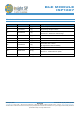
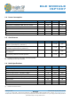
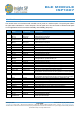
3. Pin Description
The module uses an LGA format with a double row of pads on a 0.65 mm pitch. The pad layout follows
the QFN Jedec standard for 2 row LGA parts. The NC pads are to be connected to isolated metal pads
on the application PCB for mechanical stability and reliability (drop test).
Pin
Name
Pin function
Description
1
VSS
Ground
Should be connected to ground plane on application PCB
2
P0_09
NFC1
Digital I/O
NFC Input
General purpose I/O pin
NFC antenna connection
3
P0_12
TRACEDATA1
Digital I/O
General purpose I/O pin
Trace port output
4
P0_10
NFC2
Digital I/O
NFC Input
General purpose I/O pin
NFC antenna connection
5
P0_14
Digital I/O
General purpose I/O pin
6
P0_26
Digital I/O
General purpose I/O pin
7
VSS
Ground
Should be connected to ground plane on application PCB
8
D+
Digital I/O
USB D+
9
P0_16
Digital I/O
General purpose I/O pin
10
D-
Digital I/O
USB D-
11
P0_21
Digital I/O
General purpose I/O pin
12
VBUS
Power
5V input for USB 3.3V regulator
13
P0_18
RESET
Digital I/O
General purpose I/O pin
Configurable as system RESET pin
14
VSS
Ground
Should be connected to ground plane on application PCB
15
P0_20
Digital I/O
General purpose I/O pin
16
VSS
Ground
Should be connected to ground plane on application PCB
17
P0_22
Digital I/O
General purpose I/O pin
18
VSS
Ground
Should be connected to ground plane on application PCB
19
P0_24
Digital I/O
General purpose I/O pin
20
OUT_ANT
Antenna I/O
This pin is connected to the internal antenna
It should be connected to Pin 22 OUT_MOD for normal operation
21
VSS
Ground
Should be connected to ground plane on application PCB
22
OUT_MOD
Antenna I/O
This pin is the RF I/O pin of the BLE module
It should be connected to Pin 20 OUT_ANT for normal operation
23
VSS
Ground
Should be connected to ground plane on application PCB
24
VSS
Ground
Should be connected to ground plane on application PCB
25
VSS
Ground
Should be connected to ground plane on application PCB
26
VCC_nRF
Power
Power supply (1.7 – 3.6V)
27
P0_17
Digital I/O
General purpose I/O pin
28
SWDIO
Digital I/O
Serial Wire Debug I/O for debug and programming
29
P0_13
Digital I/O
General purpose I/O pin
30
SWDCLK
Digital Input
Serial Wire Debug clock input for debug and programming
31
VSS
Ground
Should be connected to ground plane on application PCB
32
P0_08
Digital I/O
General purpose I/O pin
33
P0_07
TRACECLK
Digital I/O
General purpose I/O pin
Trace port clock output