
Datasheet

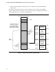
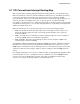

Table Of Contents
- Intel® Desktop Boards D915GEV/D915GRF Technical Product Specification
- Revision History / Disclaimer
- Preface
- Contents
- 1 Product Description
- 1.1 PCI Bus Terminology Change
- 1.2 Overview
- 1.3 Online Support
- 1.4 Processor
- 1.5 System Memory
- 1.6 Intel® 915G Chipset
- 1.7 PCI Express Connectors
- 1.8 I/O Controller
- 1.9 Audio Subsystem
- 1.10 LAN Subsystem
- 1.11 Hardware Management Subsystem
- 1.12 Power Management
- 1.12.1 ACPI
- 1.12.2 Hardware Support
- 1.12.2.1 Power Connector
- 1.12.2.2 Fan Connectors
- 1.12.2.3 LAN Wake Capabilities
- 1.12.2.4 Instantly Available PC Technology
- 1.12.2.5 Resume on Ring
- 1.12.2.6 Wake from USB
- 1.12.2.7 Wake from PS/2 Devices
- 1.12.2.8 PME# Signal Wake-up Support
- 1.12.2.9 WAKE# Signal Wake-up Support
- 1.12.2.10 +5 V Standby Power Indicator LED
- 1.13 Trusted Platform Module
- 1.13.1 System Requirements
- 1.13.2 Warning of Potential Data Loss
- 1.13.3 Security Precautions
- 1.13.4 Trusted Platform Module Ownership
- 1.13.5 Enabling the Trusted Platform Module
- 1.13.6 Assuming Trusted Platform Module Ownership
- 1.13.7 Recovery Procedures
- 1.13.8 Clearing Trusted Platform Module Ownership
- 1.13.9 Software Support
- 2 Technical Reference
- 2.1 Introduction
- 2.2 Memory Resources
- 2.3 DMA Channels
- 2.4 Fixed I/O Map
- 2.5 PCI Configuration Space Map
- 2.6 Interrupts
- 2.7 PCI Conventional Interrupt Routing Map
- 2.8 Connectors
- 2.8.1 Back Panel Connectors
- 2.8.2 Component-side Connectors
- 2.9 Jumper Block
- 2.10 Mechanical Considerations
- 2.11 Electrical Considerations
- 2.12 Thermal Considerations
- 2.13 Reliability
- 2.14 Environmental
- 2.15 Regulatory Compliance
- 3 Overview of BIOS Features
- 4 Error Messages and Beep Codes

Intel Desktop Board D915GEV/D915GRF Technical Product Specification
52
•
Memory-mapped I/O that is dynamically allocated for PCI Conventional and PCI Express
add-in cards
The amount of installed memory that can be used will vary based on add-in cards and BIOS
settings. Figure 15 shows a schematic of the system memory map. All installed system memory
can be used when there is no overlap of system addresses.
Upper BIOS
area (64 KB)
Lower BIOS
area
(64 KB;
16 KB x 4)
Add-in Card
BIOS and
Buffer area
(128 KB;
16 KB x 8)
Standard PCI/
ISA Video
Memory (SMM
Memory)
128 KB
DOS area
(640 KB)
1 MB
960 KB
896 KB
768 KB
640 KB
0 KB
0FFFFFH
0F0000H
0EFFFFH
0E0000H
0DFFFFH
0C0000H
0BFFFFH
0A0000H
09FFFFH
00000H
FLASH
APIC
Reserved
0 MB
640 KB
1 MB
Top of usable
DRAM (memory
visible to the
operating
system)
PCI Memory Range -
contains PCI, chipsets,
Direct Media Interface
(DMI), and ICH ranges
(approximately 750 MB)
DOS
Compatibility
Memory
DRAM
Range
OM17140
~20 MB
4 GB
Top of System Address Space
Figure 15. Detailed System Memory Address Map