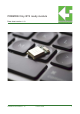
PRBMD02 tiny BT5 ready module Data sheet version 1.10 PRBMD02 DATASHEET 1.
Disclaimer Liability Disclaimer K-Solution Consulting Co. Ltd reserves the right to make changes without further notice to the product to improve reliability, function or design. K-Solution Consulting Co. Ltd does not assume any liability arising out of the application or use of any product or circuits described herein. Life Support Applications K-Solution Consulting Co.
Introduction Base on PHY+ Microelectronics’ PHY6222 Bluetooth 5 ready core chip, PRBMD02 BT 5 ready module provides a reliable and easy BT5 solution, allowing user, even without any RF design experience, brings their their product or system, embedded with BT5 feature, to market in time. Integrated with almost all peripheral components, such as RF matching network, Antenna, 16MHz Crystal, 32768Hz RC, and DC/DC inductor, which saves engineer resource from hardware design for BLE.
Hardware information PRBMD02 DATASHEET 1.
Features • 32bit CortexTM-M0 processor with 2.
Pin assignment pin 8 pin 17 pin 16 pin 24 pin 9 pin 1 pin name Description 1 GND Power ground 2 P23 GPIO 1. ADC input 1; 2. Mic bias 3 P24 GPIO ADC input 2 4 P25 GPIO ADC input 8 5 P31 GPIO 6 P32 GPIO 7 P33 GPIO 8 P34 GPIO 9 P00 GPIO 10 P01 GPIO 11 P02 GPIO SWD debug data in 12 P03 GPIO SWD debug clock 13 TM Mode select pin 14 P09 GPIO 15 P10 GPIO 16 RST RESET 17 VDD VDD, 1.8 - 3.6V 18 P14 GPIO ADC input 3 19 P15 GPIO 1. ADC input 4; 2.
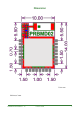
Dimension Unit: mm thickness: 3mm PRBMD02 DATASHEET 1.
Specifications (major parameters) Description Typical value Operation voltage 1.8V to 3.6V DC Operation current Advertising: Average - 3mA; Max peak - 9mA Connected Average - 3.18mA; Max peak - 9mA SLEEP mode current Sleep mode: 1uA, with 32768Hkz RTC * needed firmware activation General RF Environment Flash memory OFF mode current 0.
Radio current consumption Transmitter Description Typical Tx only at 0dBm, with internal DC-DC@3V typ. 4.6mA Rx only, with internal DC-DC@3V typ.
Description Typical Rx sensitivity, 500kbps BLE ideal transmitter, 37 Byte BER=1E-3 -96dBm co-channel rejection, modulated interferer in channel, 37 Byte BER=1E-3 -6I/C dB Selectivity +-1MH , Wanted signal at -67dBm, modulated interferer at +/- 1MHz, 37 Byte BER=1E-3 -5 I/C dB Selectivity +-2MHz Wanted signal at -67dBm, modulated interferer at the +/- 2MHz, 37 Byte BER=1E-3 9 I/C dB Selectivity +-3MHz Wanted signal at -67dBm, modulated interferer at +/- 3MHz, 37 Byte BER=1E-3 30 I/C dB Selectivi
Description Typical Rx sensitivity, 125kbps BLE ideal transmitter, 37 Byte BER=1E-3 -105 dBm co-channel rejection, modulated interferer in channel, 37 Byte BER=1E-3 -1 I/C dB Selectivity +-1MH , Wanted signal at -67dBm, modulated interferer at +/- 1MHz, 37 Byte BER=1E-3 -11 I/C dB Selectivity +-2MHz Wanted signal at -67dBm, modulated interferer at the +/- 2MHz, 37 Byte BER=1E-3 45 I/C dB Selectivity +-3MHz Wanted signal at -67dBm, modulated interferer at +/- 3MHz, 37 Byte BER=1E-3 50 I/C dB Sele
Reset the module The reset pin connection could be one of the following: optional optional 3.3VDC 3.3VDC 10k 10k MCU reset power up reset 1uF 1uF 1uF reset reset push button reset circuit reset by MCU Reset pin contains internal pull up, and external pull up circuit is optional. A low signal will reset the module, and the timing is illustrated as following: Reset to tr module enters operation tr = at least 1µs to = 500µs PRBMD02 DATASHEET 1.
9mm The clock Main clock PRBMD02 embeds with a 16MHz main oscillator, and it is software configurable up scale to higher internal frequency: 32M, 48M, 64M or 96MHz. By default it is not up scaled. P02 P01 P25 P31 3.3V P03 P09/TX GND TM GND 20PF PRMBD01 front view, with shielding RTC If 32.768kHz crystal is not installed (pin P16 and P17), internal RC oscillator circuit can be then enable by firmware and be use as real time clock.
Firmware programming User is able to program their own developed firmware (with SDK) into PRBMD0x. The programming procedure is as following, programming software, PhyPlusKit.exe (for window) must be pre-installed, and UART-USB dongle may be needed: 1. 2. 3. 4. 5. 6. Connect TM pin (pin 10) to 3.
GPIO and interfaces Every GPIO can be configured as Input, Output and Interrupt, and can also be configured as weak pull-up, strong pull-up, weak pull-low or floating mode. Except ADC, all interfaces are possible to map to different GPIOs by software. The interface including: 1. I2C: it supports 100KHz and 400KHz modes, 7-bit and 10-bit address 2. I2S: either master or slave mode can be enabled 3. UART: Asynchronous Rx/Tx, up to almost 1Mbps, supports parity and 9 bit-data 4.
RF characteristic PRBMD02 RF characteristic is illustrated as following: PRBMD02 DATASHEET 1.
PRBMDxx family comparison PRBMD00 PRBMD02 Core chip Cortex ™ -M0 Cortex ™ -M0 with SWD Dimension 12x18mm 10x14mm # of GPIO 33 GPIOs 19 GPIOs Operation voltage 2.5 - 6V 1.8-3.
Points to note • IO pins pull high/low resistance: - Floating: Hi-Z - Strong pull up: 150KΩ - Weak pull up: 1MΩ - Pull down: 100kΩ • P1, P15, P16, P17 do not support FullMUX, and only treated as GPIO. • Except TM/ P16 and P17, all GPIO support interrupt and wakeup • Single-end ADC pins: P11, P23, P24, P14 and P15 • Differential ADC pins: P18-P25; P14-P24; P20-P15 • Two modes available for ADC: bypass and attenuation: - By-pass mode Without attenuation, input range should be 0-0.
Firmware information PRBMD02 DATASHEET 1.
Default firmware PRBMD02 comes with default UART-BT firmware, allowing user able to enable their product with BT feature without any extra engineer resources. The firmware basic feature is to tunnel data between UART port and Bluetooth device (Transparent mode). User can develop their own firmware by SDK as well if default firmware is not applicable. AT-CMD and Transparent Modes The firmware contains two modes: AT-CMD mode and Transparent mode.
Mode switching The switching between AT-CMD and Transparent mode is automatically. When PRBMD02 is NOT connected with smartphone, tablet…, PRBMD02 will enter AT-CMD mode and AT-command will be accepted from UART port; and once PRBMD02 is connected to with smartphone or any other BT device, PRBMD02 will automatically go into Transparent mode, and all data from UART, even AT-CMD, will be treated as data and send out to BT side.
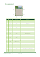
AT-command AT-command in AT-CMD mode are listed as below: BT related UART and GPIO Action enquiry return value set set/get ID AT+ID? Current address AT+ID=addr addr format: xx:xx:xx:xx:xx:xx Help AT+HELP List all AT commands and status Reset AT+RESET Factory Default setting (reset needed) AT+DEFAULT Change name AT+NAME ? - current name Default:PRBMD02 AT+BDCS Stop advertising AT+BDCE Get/Set Tx power level AT+TXP? 0-4 0: 5dBm 1: 0dBm 2: -5dBm 3: -20dBm 4: -10dBm AT+TXP=y y= 0-4 B
Firmware programming Tx Rx 3.3V USB-UART dongle Note: Some USB-UART dongle may have different definition of Tx and Rx, can swap these pins if not success PhyPlusKit interface Note: More information will be described in PRBMD0x Programming document. MAC address Unless otherwise instructed, each PRBMD02 will be shipped with KATP preprogrammed but no MAC address is pre-programmed. User can program their own MAC address by PhyPlusKit.
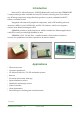
Mounting guide PRBMD02 is RF sensitive; in order to obtain the best performance, it is recommended to mount the module at corner of mother board, and with some marginal space. Also, keep it away from metal components, such like speakers, transformers, batteries, big aluminum capacitors, heat sinks and Metal Panels. The figure below illustrates how to mount the PRBMD02 module. Improper mounting will decrease the RF performance dramatically. PRBMD02 PRBMD02 DATASHEET 1.
Evaluation Board Evaluation board (EVB) is available, helping engineer for the firmware development. It is in DIP form factor, allows engineer to connect with external circuit easily for debugging and testing. EVB for PRBMD02 is same as EVB for PRBMD00, and an adaptor board that convert PRBMD02 pin to connect with the EVB The EVB is illustrated as following: 50mm PRBMD02 on adaptor board 30mm The EVK is in DIP format with PRBMD02 (and adaptor board) on it, and with on board 32.
USB-UART LED TM jumper module LED Reset button VBUS 1. 32K jumper: Since P16,P17 are multiplex with external 32.768KHz oscillator, this jumper allows the PRBMD02 to connected with the on board 32.768KHz oscillator. 2. LED & UART jumper: This jumper allows the module to connected with on-board LED and the on-board USB-UART chip. Connecting 5V allow PRBMD02 to be powered from USB. Connecting 3V3 will provides a 3.3VDC to the rest of the board 3.
PRBMD02 DATASHEET 1.
Firmware development and SDK User is allowed to developed their own firmware for PRBMD02 through SDK as following: 1. copy SDK to a working directory 2. install MDK Keil5 for ARM IDE 3. Example code in SDK can now be edit and compiled. Experience on ARM core firmware development will be very helpful for development the firmware.
Service Firmware programming K-Solution provide pre-programming service, so that PRBMD02 will be shipped with firmware pre-programmed. Service charge is needed. Software service from K-Solution K-Solution also provides firmware develop service for PRBMD02 module, hence customer do not need to spend their resource on the firmware development. These services requires NRE charge. For the details, please contact our local sales representative or distributor.
Certifications PRBMD02 DATASHEET 1.
Ordering part number PR BM D xx - XXX optional, Pre-program firmware number module model version Application: D-IoT, A-Audio Wireless technology Products Prefix Available part number: PRBMD00 - PHY6212 core BT5 module, on board chip antenna, 38 pins, 12 x 18 mm, standard UART firmware, chip antenna, metal shielding and certifications PRBMD01 - PHY6212 core BT5 module, on board chip antenna, 38 pins, 12 x 18 mm standard UART firmware, chip antenna, no metal shielding and no certification, on board DC-DC
PRBMD00 label PRBMD00 label Label 9mm 9mm hardware version, including PCB and components K-SolutionConsulting Consulting K-Solution PRBMD00 PRBMD02 PRBMD00 HWver: ver:1.0 1.0 FM FMversion:0.0 version:0.0 HW date:202116 202116 date: FCCID: ID:2AX9WMD00 2AX9WMD02 FCC 8.8mm 10mm 10mm Production lot Certification information d e t a d p b u e Note: label design may be update and modified if needed o T PRBMD02 DATASHEET 1.
Conformity FCC regulatory conformance: This device complies with Part 15 of the FCC Rules. Operation is subject to the following two conditions: (1) This device may not cause harmful interference. (2) This device must accept any interference received, including interference that may cause undesired operation. NOTE: This equipment has been tested and found to comply with the limits for a Class B digital device, pursuant to part 15 of the FCC Rules.
ORIGINAL EQUIPMENT MANUFACTURER (OEM) NOTES The OEM must certify the final end product to comply with unintentional radiators (FCC Sections 15.107 and 15.109) before declaring compliance of the final product to Part 15 of the FCC rules and regulations. Integration into devices that are directly or indirectly connected to AC lines must add with Class II Permissive Change. The OEM must comply with the FCC labeling requirements.
Operating Frequency:(Bluetooth LE)2402-2480MHz RF output power(Max):-3.08dBm Manufacturer information: Company name: K-Solution Consulting Co. Ltd Address:Blk. H, 11/f, Yuet Wah mansion, 39 Yuet Wah street, KwunTong, HK CAUTION: 1. EUT Temperature: 0℃~+50℃. 2. Input: DC 3.3V 3. The device complies with RF specifications when the device used at 5 mm from your body, and the holder must not be of metal composition.
Package Standard package of PRBMD02 is anti-electro static plastic tray, where each tray should able to contain xx pcs PRBMD02. Dimension of each tray is xxxx mm. d te o T b u e a d p Note: package format is subject to change in order to enhance the efficiency PRBMD02 DATASHEET 1.
PRBMD0x comparison PRBMD00 PRBMD01 PRBMD02 PRBMD03 PRBMD12 Core chip PHY6212 PHY6212 PHY6222 PHY6222 PHY6222 MCU core M0 M0 M0 M0 M0 RAM (Byte) 138K 138K 64K 64K 64K FLASH (Byte) 512K 512K 128K 128K 128K Cache (Byte) 0 0 8K 8K 8K available available available available available 5.2 5.2 5.2 5.2 5.
PRBMD0x power consumption test result The following is are power consumption testing result of PRBMD0x under different conditions. testing condition model EVK with SDK 3.
Revision History 2021-03-02 2021-12-16 2022-04-01 version 0.5 version 0.9 version 0.99 INTEGRATION TO THE END PRODUCT The Transceiver Module, model 2AX9WMD02 has to be installed and used in accordance with the technical description/installation instructions provided by the manufacturer. Integration instructions for host product manufacturers according to KDB 996369 D03 OEM Manual v01 2.2 List of applicable FCC rules CFR 47 FCC PART 15 SUBPART C has been investigated.
Reference ADC Application Note ANCS Application Note Font Application Note GPIO Application Note OTA Note SDK Application Guide MESH Application Guide KATP product brief PRBMD02 DATASHEET 1.
Contact information Head quarter: K-Solution Consulting Co. Ltd. web: www.k-sol.com.hk Tel: +852-91983405 Fax: +852 3013 8763 E-mail: sales@k-sol.com.hk PRBMD02 DATASHEET 1.