
Datasheet


SMU INSTRUMENTS
www.keithley.com
1.888.KEITHLEY
(U.S. only)
A Greater Measure of Confidence
2634B, 2635B,
2636B
System SourceMeter
®
SMU Instruments
METER SPECIFICATIONS (continued)
NOTES
16. Add 50µV to source accuracy specifications per volt of HI lead drop.
17. De-rate accuracy specifications for NPLC setting <1 by increasing error term. Add appropriate % of range term
using table below.
NPLC Setting
200mV
Range
2V–200V
Ranges
100nA
Range
1µA–100mA
Ranges
1A–1.5A
Ranges
0.1 0.01% 0.01% 0.01% 0.01% 0.01%
0.01 0.08% 0.07% 0.1% 0.05% 0.05%
0.001 0.8 % 0.6 % 1% 0.5 % 1.1 %
18. Applies when in single channel display mode.
19. High Capacitance Mode accuracy is applicable at 23°C ±5°C only.
20. Applies when in single channel display mode.
21. Four-wire remote sense only and with current meter mode selected. Voltage measure set to 200mV or
2V range only.
22. 10-NPLC, 11-Point Median Filter, <200V range, measurements made within 1 hour after zeroing. 23°C ± 1°C
23. Under default specification conditions: ±(0.15% + 750fA).
24. Under default specification conditions: ±(0.15% + 1pA).
25. 10A range accessible only in pulse mode.
26. Delay factor set to 1. Compliance equal to 100mA.
27. High Capacitance Mode accuracy is applicable at 23°C ±5°C only.
28. Includes measurement of SENSE HI to HI and SENSE LO to LO contact resistances.
HIGH CAPACITANCE MODE
29, 30, 31
VOLTAGE SOURCE OUTPUT SETTLING TIME: Time required to reach within 0.1% of final value
after source level command is processed on a fixed range. Current limit = 1A.
Voltage Source Range Settling Time with C
load
= 4.7µF
200 mV 600 µs (typical)
2 V 600 µs (typical)
20 V 1.5 ms (typical)
200 V 20 ms (typical)
CURRENT MEASURE SETTLING TIME: Time required to reach within 0.1% of final value after
voltage source is stabilized on a fixed range. Values below for V
out
= 2V unless noted.
Current Measure Range Settling Time
1.5 A – 1 A <120 µs (typical) (R
load
>6W)
100 mA – 10 mA <100 µs (typical)
1 mA < 3 ms (typical)
100 µA < 3 ms (typical)
10 µA < 230 ms (typical)
1 µA < 230 ms (typical)
CAPACITOR LEAKAGE PERFORMANCE USING HIGH-C SCRIPTS
32
: Load = 5µF||10MW.
Test: 5V step and measure. 200ms (typical) @ 50nA.
MODE CHANGE DELAY:
100µA Current Range and Above:
Delay into High Capacitance Mode: 10ms.
Delay out of High Capacitance Mode: 10ms.
1µA and 10µA Current Ranges:
Delay into High Capacitance Mode: 230ms.
Delay out of High Capacitance Mode: 10ms.
VOLTMETER INPUT IMPEDANCE: 30GW in parallel with 3300pF.
NOISE, 10Hz–20MHz (20V Range): <30mV peak-peak (typical).
VOLTAGE SOURCE RANGE CHANGE OVERSHOOT (for 20V range and below): <400mV + 0.1%
of larger range (typical). Overshoot into a 200kW load, 20MHz BW.
NOTES
29. High Capacitance Mode specifications are for DC measurements only.
30. 100nA range and below are not available in high capacitance mode.
31. High Capacitance Mode utilizes locked ranges. Auto Range is disabled.
32. Part of KI Factory scripts. See reference manual for details.
GENERAL
IEEE-488: IEEE-488.1 compliant. Supports IEEE-488.2 common commands and status
model topology.
USB CONTROL (REAR): USB 2.0 device, TMC488 protocol.
RS-232: Baud rates from 300bps to 115200bps. Programmable number of data bits, parity
type, and flow control (RTS/CTS hardware or none).
ETHERNET: RJ-45 connector, LXI Class C, 10/100BT, no auto MDIX.
EXPANSION INTERFACE: The TSP-Link expansion interface allows TSP enabled instruments
to trigger and communicate with each other. (Not available on Model 2614B.)
Cable Type: Category 5e or higher LAN crossover cable.
Length: 3 meters maximum between each TSP enabled instrument.
LXI COMPLIANCE: LXI Class C 1.4.
LXI TIMING: Total Output Trigger Response Time: 245µs min., 280µs typ., (not
specified) max. Receive LAN[0-7] Event Delay: Unknown. Generate LAN[0-7] Event
Delay: Unknown.
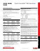
DIGITAL I/O INTERFACE: (Not available on Model 2614B)
+5VDC
5.1kΩ
100Ω
Solid State
Fuse
Read by
firmware
Written by
firmware
+5V Pins
(on DIGITAL I/O
connector)
Dig
ital I/O Pin
(on DIGITAL I/O
connector)
GND Pin
(on DIGITAL I/O
connector)
Rear Panel
Connector: 25-pin female D.
Input/Output Pins: 14 open drain I/O bits.
Absolute Maximum Input Voltage: 5.25V.
Absolute Minimum Input Voltage: –0.25V.
Maximum Logic Low Input Voltage: 0.7V, +850µA max.
Minimum Logic High Input Voltage: 2.1V, +570µA.
Maximum Source Current (flowing out of Digital I/O bit): +960µA.
Maximum Sink Current @ Maximum Logic Low Voltage (0.7V): –5.0mA.
Absolute Maximum Sink Current (flowing into Digital I/O pin): –11mA.
5V Power Supply Pins: Limited to 250mA total for all three pins, solid state fuse protected.
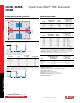
Safety Interlock Pin: Active high input. >3.4V @ 24mA (absolute maximum of 6V) must
be externally applied to this pin to ensure 200V operation. This signal is pulled down
to chassis ground with a 10kW resistor. 200V operation will be blocked when the
INTERLOCK signal is <0.4V (absolute minimum –0.4V). See figure below:
*
10kΩ
Coil
Resistance
145Ω ±10%
Read by firmware
INTERLOCK Pin
(on DIGITAL I/O
connector)
Rear Panel
Chassis
Ground
To output stage
+220V Supply
–220V Supply
USB FILE SYSTEM (FRONT): USB 2.0 Host: Mass storage class device.
POWER SUPPLY: 100V to 250VAC, 50–60Hz (auto sensing), 240VA max.
COOLING: Forced air. Side intake and rear exhaust. One side must be unobstructed when
rack mounted.
EMC: Conforms to European Union Directive 2004/108/EEC, EN 61326-1.
SAFETY: Conforms to European Union Directive 73/23/EEC, EN 61010-1, and UL 61010-1.
DIMENSIONS: 89mm high × 213mm wide × 460mm deep (3½ in × 8
3
⁄
8
in × 17½ in). Bench
Configuration (with handle and feet): 104mm high × 238mm wide × 460mm deep (4
1
⁄
8
in
× 9
3
⁄
8
in × 17½ in).
WEIGHT: 2635B: 4.75kg (10.4 lbs). 2634B, 2636B: 5.50kg (12.0 lbs).
ENVIRONMENT: For indoor use only. Altitude: Maximum 2000 meters above sea level.
Operating: 0°–50°C, 70% R.H. up to 35°C. Derate 3% R.H./°C, 35°–50°C.
Storage: –25°C to 65°C.
SEE PAGES 23 AND 24 FOR MEASUREMENT
SPEEDS AND OTHER SPECIFICATIONS.
Series 2600B specifications
Series 2600B specifications