
Datasheet

LT1073
4
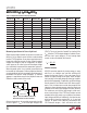
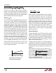
TYPICAL PERFOR A CE CHARACTERISTICS
UW
Supply Current vs Temperature
Recommended Minimum
Inductance Value
Guaranteed Minimum Output
Current at 5V vs V
IN
UU
U
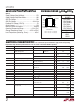
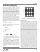
PI FU CTIO S
I
LIM
(Pin 1): Connect this pin to V
IN
for normal use. Where
lower current limit is desired, connect a resistor between
I
LIM
and V
IN
. A 220Ω resistor will limit the switch current
to approximately 400mA.
V
IN
(Pin 2): Input Supply Voltage
SW1 (Pin 3): Collector of Power Transistor. For step-up
mode connect to inductor/diode. For step-down mode
connect to V
IN
.
SW2 (Pin 4): Emitter of Power Transistor. For step-up
mode connect to ground. For step-down mode connect to
inductor/diode. This pin must never be allowed to go more
than a Schottky diode drop below ground.
GND (Pin 5): Ground.
AO (Pin 6): Auxiliary Gain Block (GB) Output. Open collec-
tor, can sink 100µA.
SET (Pin 7): GB Input. GB is an op amp with positive input
connected to SET pin and negative input connected to
212mV reference.
FB/SENSE (Pin 8): On the LT1073 (adjustable) this pin
goes to the comparator input. On the LT1073-5 and
LT1073-12, this pin goes to the internal application resis-
tor that sets output voltage.
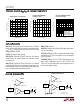
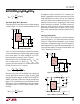
BLOCK DIAGRA S
W
LT1073
LT1073-5 and LT1073-12
TEMPERATURE (°C)
–50
SUPPLY CURRENT (µA)
100
1073 G07
050
150
140
130
120
110
100
90
80
70
60
50
–25 25 75 125
V
IN
= 1.5V
INPUT VOLTAGE (V)
MINIMUM INDUCTANCE (µH)
1073 G08
300
250
200
150
100
50
0
1.0
2.0
3.0
3.5
1.5 2.5
4.0
4.5
5.0
R
LIM
= 0V
V
IN
(V)
1.0
OUTPUT CURRENT (mA)
1000
100
10
1.5 2.0 2.5 3.0 3.5
1073 G09
FOR V
IN
> 1.6V A
68Ω RESISTOR
MUST BE CONNECTED
BETWEEN I
LIM
AND V
IN
–
+
A1
A2
COMPARATOR
DRIVER
212mV
REFERENCE
OSCILLATOR
GAIN BLOCK/ERROR AMP
V
IN
SET
A0
I
LIM
SW1
Q1
SW2
FB
GND
1073 BD01
–
+
A1
A2
COMPARATOR
DRIVER
212mV
REFERENCE
OSCILLATOR
GAIN BLOCK/ERROR AMP
V
IN
SET
A0
I
LIM
SW1
Q1
SW2
GND
1073 BD02
R1
R2
940k
SENSE
LT1073-5: R1 = 40k
LT1073-12: R2 = 16.3k