
Datasheet


LT1083/LT1084/LT1085
5
108345fg
Note 1: Stresses beyond those listed under Absolute Maximum Ratings
may cause permanent damage to the device. Exposure to any Absolute
Maximum Rating condition for extended periods may affect device
reliability and lifetime.
Note 2: See thermal regulation specifi cations for changes in output voltage
due to heating effects. Load and line regulation are measured at a constant
junction temperature by low duty cycle pulse testing.
Note 3: Line and load regulation are guaranteed up to the maximum power
dissipation (60W for the LT1083, 45W for the LT1084 (K, P), 30W for the
LT1084 (T) and 30W for the LT1085). Power dissipation is determined by
the input/output differential and the output current. Guaranteed maximum
power dissipation will not be available over the full input/output voltage
range.
Note 4: I
FULL_LOAD
is defi ned in the current limit curves. The I
FULL_LOAD
curve is defi ned as the minimum value of current limit as a function of
input-to-output voltage. Note that the 60W power dissipation for the
LT1083 (45W for the LT1084 (K, P), 30W for the LT1084 (T), 30W for the
LT1085) is only achievable over a limited range of input-to-output voltage.
Note 5: Dropout voltage is specifi ed over the full output current range of
the device. Test points and limits are shown on the Dropout Voltage
curve.
Note 6: For LT1083 I
FULL_LOAD
is 5A for –55°C ≤ T
J
< – 40°C and 7.5A for
T
J
≥ –40°C.
Note 7: 1.7V ≤ (V
IN
– V
OUT
) ≤ 25V for LT1084 at –55°C ≤ T
J
≤ – 40°C.
Note 8: Dropout is 1.7V maximum for LT1084 at –55°C ≤ T
J
≤ –40°C.
Note 9: The LT1083/LT1084/LT1085 regulators are tested and specifi ed
under pulse load conditions such that T
J
≅ T
A
. The C-grade LT1083/
LT1084/LT1085 are 100% tested at 25°C.The I-grade LT1084/LT1085 are
guaranteed over the full –40°C to 125°C operating ambient temperature
range.
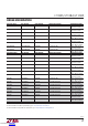
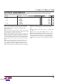
ELECTRICAL CHARACTERISTICS
The l denotes the specifi cations which apply over the full operating
temperature range, otherwise specifi cations are at T
A
= 25°C.
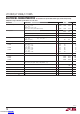
PARAMETER CONDITIONS MIN TYP MAX UNITS
Thermal Resistance Junction-to-Case
LT1083
LT1084
LT1085
Control Circuitry/Power Transistor
K Package
P Package
K Package
P Package
T Package
K Package
M, T Package
0.6/1.6
0.5/1.6
0.75/2.3
0.65/2.3
0.65/2.7
0.9/3.0
0.7/3.0
°C/W
°C/W
°C/W
°C/W
°C/W
°C/W
°C/W
Downloaded from Arrow.com.Downloaded from Arrow.com.Downloaded from Arrow.com.Downloaded from Arrow.com.Downloaded from Arrow.com.