
Datasheet

10
LT1360
APPLICATIONS INFORMATION
WUU
U
Capacitive Loading
The LT1360 is stable with any capacitive load. This is
accomplished by sensing the load induced output pole
and adding compensation at the amplifier gain node. As
the capacitive load increases, both the bandwidth and
phase margin decrease so there will be peaking in the
frequency domain and in the transient response as shown
in the typical performance curves.The photo of the small-
signal response with 500pF load shows 60% peaking. The
large-signal response with a 10,000pF load shows the
output slew rate being limited to 5V/µs by the short-circuit
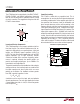
current. Coaxial cable can be driven directly, but for best
pulse fidelity a resistor of value equal to the characteristic
impedance of the cable (i.e., 75Ω) should be placed in
series with the output. The other end of the cable should
be terminated with the same value resistor to ground.
Cable Driver Frequency Response
FREQUENCY (MHz)
1
–8
–6
–4
–2
0
GAIN (dB)
2
100
1360 AI02
10
A
V
= 2
R
F
= R
G
= 500Ω
R
L
= 150Ω
V
S
= ±10V
V
S
= ±5V
V
S
= ±2.5V
V
S
= ±15V
–
+
LT1360
510Ω
75Ω
OUT
75Ω
IN
510Ω
The LT1360 may be inserted directly into AD817, AD847,
EL2020, EL2044, and LM6361 applications improving
both DC and AC performance, provided that the nulling
circuitry is removed. The suggested nulling circuit for the
LT1360 is shown below.
Offset Nulling
1360 AI01
6
7
V
+
V
–
4
8
1
2
10k
3
–
+
LT1360
Layout and Passive Components
The LT1360 amplifier is easy to apply and tolerant of less
than ideal layouts. For maximum performance (for ex-
ample fast settling time) use a ground plane, short lead
lengths, and RF-quality bypass capacitors (0.01µF to
0.1µF). For high drive current applications use low ESR
bypass capacitors (1µF to 10µF tantalum). Sockets
should be avoided when maximum frequency perfor-
mance is required, although low profile sockets can
provide reasonable performance up to 50MHz. For
more details see Design Note 50.
The parallel combination of the feedback resistor and gain
setting resistor on the inverting input can combine with
the input capacitance to form a pole which can cause
peaking or oscillations. For feedback resistors greater
than 5kW, a parallel capacitor of value
C
F
> R
G
x C
IN
/R
F
should be used to cancel the input pole and optimize
dynamic performance. For unity-gain applications where
a large feedback resistor is used, C
F
should be greater
than or equal to C
IN
.