
Datasheet


12
LT1360
Circuit Operation
The LT1360 circuit topology is a true voltage feedback
amplifier that has the slewing behavior of a current feed-
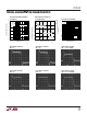
back amplifier. The operation of the circuit can be under-
stood by referring to the simplified schematic. The inputs
are buffered by complementary NPN and PNP emitter
followers which drive a 500Ω resistor. The input voltage
appears across the resistor generating currents which are
mirrored into the high impedance node. Complementary
followers form an output stage which buffers the gain
node from the load. The bandwidth is set by the input
resistor and the capacitance on the high impedance node.
The slew rate is determined by the current available to
charge the gain node capacitance. This current is the
differential input voltage divided by R1, so the slew rate is
proportional to the input. Highest slew rates are therefore
seen in the lowest gain configurations. For example, a 10V
output step in a gain of 10 has only a 1V input step,
whereas the same output step in unity gain has a 10 times
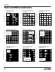
greater input step. The curve of Slew Rate vs Input Level
illustrates this relationship. The LT1360 is tested for slew
rate in a gain of –2 so higher slew rates can be expected
in gains of 1 and –1, and lower slew rates in higher gain
configurations.
The RC network across the output stage is bootstrapped
when the amplifier is driving a light or moderate load and
has no effect under normal operation. When driving a
capacitive load (or a low value resistive load) the network
is incompletely bootstrapped and adds to the compensa-
tion at the high impedance node. The added capacitance
slows down the amplifier which improves the phase
margin by moving the unity-gain frequency away from the
pole formed by the output impedance and the capacitive
load. The zero created by the RC combination adds phase
to ensure that even for very large load capacitances, the
total phase lag can never exceed 180 degrees (zero phase
margin) and the amplifier remains stable.
Comparison to Current Feedback Amplifiers
The LT1360 enjoys the high slew rates of Current Feed-
back Amplifiers (CFAs) while maintaining the characteris-
tics of a true voltage feedback amplifier. The primary
differences are that the LT1360 has two high impedance
inputs and its closed loop bandwidth decreases as the gain
increases. CFAs have a low impedance inverting input and
maintain relatively constant bandwidth with increasing
gain. The LT1360 can be used in all traditional op amp
configurations including integrators and applications such
as photodiode amplifiers and I-to-V converters where
there may be significant capacitance on the inverting
input. The frequency compensation is internal and not
dependent on the value of the feedback resistor. For CFAs,
the feedback resistance is fixed for a given bandwidth and
capacitance on the inverting input can cause peaking or
oscillations. The slew rate of the LT1360 in noninverting
gain configurations is also superior in most cases.
APPLICATIONS INFORMATION
WUU
U