
Datasheet
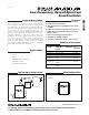

DS1090
Low-Frequency, Spread-Spectrum
EconOscillator
2 _____________________________________________________________________
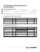
ABSOLUTE MAXIMUM RATINGS
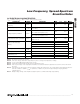
RECOMMENDED DC OPERATING CONDITIONS
(T
A
= -40°C to +85°C)
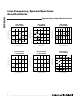
DC ELECTRICAL CHARACTERISTICS
(V
CC
= +3.0V to +5.5V, T
A
= -40°C to +85°C, unless otherwise noted.)
Stresses beyond those listed under “Absolute Maximum Ratings” may cause permanent damage to the device. These are stress ratings only, and functional
operation of the device at these or any other conditions beyond those indicated in the operational sections of the specifications is not implied. Exposure to
absolute maximum rating conditions for extended periods may affect device reliability.
Voltage Range on V
CC
Relative to Ground ...........-0.5V to +6.0V
Voltage Range on Input Pins
Relative to Ground.................................-0.5V to (V
CC
+ 0.5V),
not to exceed 6.0V
Operating Temperature Range ...........................-40°C to +85°C
Storage Temperature Range .............................-55°C to +125°C
Soldering Temperature .......................................See IPC/JEDEC
J-STD-020A Specification
PARAMETER SYMBOL CONDITIONS MIN TYP MAX UNITS
Supply Voltage V
CC
(Note 1) 3.0 5.5 V
Input Logic 1 (J0, J1, JC0, JC1) V
IH
0.7 x
V
CC
V
CC
+
0.3
V
Input Logic 0 (J0, J1, JC0, JC1) V
IL
-0.3
+0.3 x
V
CC
V
PARAMETER SYMBOL CONDITIONS MIN TYP MAX UNITS
C
L
= 15pF, V
CC
= 3.3V, R
SET
= 40kΩ 1.4
Supply Current I
CC
C
L
= 15pF, V
CC
= 5.5V, R
SET
= 40kΩ 1.7 3
mA
I
OH
= -4mA
High-Level Output Voltage (OUT) V
OH
V
CC
= min
2.4 V
Low-Level Output Voltage (OUT) V
OL
I
OL
= 4mA 0.4 V
High-Level Input Current
(J0, J1, JC0, JC1)
I
IH
V
IH
= V
CC
+1.0 µA
Low-Level Input Current
(J0, J1, JC0, JC1)
I
IL
V
IL
= 0V -1.0 µA
Resistor Current I
RES
V
CC
= max 150 µA