
Datasheet
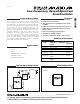

DS1090
Low-Frequency, Spread-Spectrum
EconOscillator
_____________________________________________________________________ 3
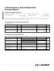
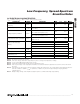
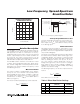
PARAMETER SYMBOL CONDITIONS MIN TYP MAX UNITS
Internal Master Oscillator
Frequency
f
MOSC
4.0 8.0 MHz
Output Frequency Tolerance f
OUT
V
CC
= 3.3V,
T
A
= +25°C
-3.0 +3.0 %
T
A
= +25°C, R
SET
= 60k,
V
CC
= 3.0V to 3.6V (Notes 2, 3)
-0.5 +0.5
Voltage Frequency Variation f
OUT
T
A
= +25°C, R
SET
= 60k,
V
CC
= 4.5V to 5.5V (Notes 2, 3)
-1.25 +1.25
%
Temperature Frequency Variation f
OUT
V
CC
= 3.3V
(Notes 2, 3, 4)
-2.0 +2.0 %
J0 = GND, J1 = GND 0
J0 = V
CC
, J1 = GND 2
J0 = GND, J1 = V
CC
4
Peak-to-Peak Dither (3)
(Note 5)
J0 = V
CC
, J1 = V
CC
8
%
Power-Up Time
t
POR
+
t
STAB
(Note 6) 0.1 0.5 ms
Load Capacitance C
L
(Note 7) 30 pF
4MHz to 8MHz, T
A
= +25°C (Note 3) 45 55
Output Duty Cycle
<4MHz (Note 4) 50
%
Output Rise/Fall Time t
R
, t
F
C
L
= 15pF 20 ns
AC ELECTRICAL CHARACTERISTICS
(V
CC
= +3.0V to +5.5V, T
A
= -40°C to +85°C, unless otherwise noted.)
Note 1: All voltages referenced to ground.
Note 2: This is the change observed in output frequency due to changes in temperature or voltage.
Note 3: See the Typical Operating Characteristics section.
Note 4: Parameter is guaranteed by design and is not production tested.
Note 5: This is a percentage of the output period. Parameter is characterized but not production tested. This can be varied from
0% to 8%.
Note 6: This indicates the time between power-up and the outputs becoming active. An on-chip delay is intentionally introduced to
allow the oscillator to stabilize. t
STAB
is equivalent to ~500 clock cycles and is dependent upon the programmed
output frequency.
Note 7: Output voltage swings can be impaired at high frequencies combined with high output loading.