
User`s guide


PCIe-DIO24 User's Guide Introducing the PCIe-DIO24
6
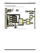
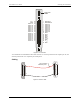
Functional block diagram
PCIe-DIO24 functions are illustrated in the block diagram shown here.
Figure 1. PCIe-DIO24 functional block diagram
Boot
EEPROM
37-pin I/O Connector
Fuse
Protection
8
8
4
4
8
PORT A
PCI-to-Local
Bus
BADR2
+
BADR3
Bus
Timing
LAD(0:7)
8
PCI Express Edge Connector
x1 Link
PCIe-to-PCI
Bridge
PCI Bus
3.3V
3.3V
1.5V
Regulator
3.3V, 32-bit, 66 MHz
+V
Regulated
DIO
Local
Address
&
Data Bus
3.3V Board Power
Interface
Decode/Status
82C55 Emulation
Logic, Control,
Complex,
Programmable
Logic Device
(CPLD)
User
3.3/5V
I/O Switch
5V
(VDD)
3.3 V
PORT A
Buffering
3.3/5V
Direction CTR
PORT B
Buffering
PORT CL
Buffering
PORT CH
Buffering
PORT B
3.3/5V
Direction CTR
8
PORT CL
3.3/5V
Direction CTR
4
PORT CH
3.3/5V
Direction CTR
4
24
4
Direction
Control
GND
4
EEPROM
switch
+5V (VDD)
10 k
Pull
Resistor
Network
Ω
Buffer
4
Spare Fuse
V and 12V
DIO
+V
(pin 18)
DIO
+V
DIO
(pin 20)
+12V
(pin 16)
IRQ Input
IRQ Enable
+5 (VDD)
5V
Regulator
Fuse
Protection
+12V
V
DIO