PCI-2513 User's Guide Document Revision 6, December, 2010 © Copyright 2010, Measurement Computing Corporation
Your new Measurement Computing product comes with a fantastic extra — Management committed to your satisfaction! Thank you for choosing a Measurement Computing product—and congratulations! You own the finest, and you can now enjoy the protection of the most comprehensive warranties and unmatched phone tech support. It’s the embodiment of our mission: To provide PC-based data acquisition hardware and software that will save time and save money.
Table of Contents Preface About this User's Guide .......................................................................................................................6 What you will learn from this user's guide ......................................................................................................... 6 Conventions in this user's guide ......................................................................................................................... 6 Where to find more information .
PCI-2513 User's Guide Using detection setpoints for output control ..................................................................................................... 27 What are detection setpoints? ..........................................................................................................................................27 Setpoint configuration overview ......................................................................................................................................
Preface About this User's Guide What you will learn from this user's guide This user's guide explains how to install, configure, and use the PCI-2513 so that you get the most out of its analog input, digital I/O, and counter/timer I/O features. This user's guide also refers you to related documents available on our web site and to technical support resources.
Chapter 1 Introducing the PCI-2513 Overview: PCI-2513 features The PCI-2513 is supported under popular Microsoft® Windows® operating systems. The PCI-2513 provides either eight differential or 16 single-ended analog inputs with 16-bit resolution. It offers seven software-selectable analog input ranges of ±10 V, ±5 V, ±2 V, ±1 V, ±0.5 V, ±0.2 V, and ±0.1V. The board has 24 high-speed lines of digital I/O, two timer outputs, and four 32-bit counters.
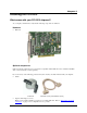
Chapter 2 Installing the PCI-2513 What comes with your PCI-2513 shipment? As you unpack your PCI-2513, verify that the following components are included. Hardware PCI-2513 Optional components Cables and signal conditioning accessories that are compatible with the PCI-2513 are not included with PCI2513 orders, and must be ordered separately. If you ordered any of the following products with your board, they should be included with your shipment.
PCI-2513 User's Guide Installing the PCI-2513 Additional documentation In addition to this hardware user's guide, you should also receive the Quick Start Guide (available in PDF at www.mccdaq.com/PDFmanuals/DAQ-Software-Quick-Start.pdf). This booklet supplies a brief description of the software you received with your PCI-2513 and information regarding installation of that software. Please read this booklet completely before installing any software or hardware.
PCI-2513 User's Guide 3. Installing the PCI-2513 To test your installation and configure your board, run the InstaCal utility installed in the previous section. Refer to the Quick Start Guide shipped with the board for information on how to initially set up and load InstaCal. If your board has been powered-off for more than 10 minutes, allow your computer to warm up for at least 30 minutes before acquiring data. This warm-up period is required in order for the board to achieve its rated accuracy.
PCI-2513 User's Guide Installing the PCI-2513 Connector pinout 16-channel single-ended mode pinout (8-channel differential signals in parentheses) Signal name Pin Pin Signal name ACH0 (ACH0 HI) AGND ACH9 (ACH1 LO) ACH2 (ACH2 HI) AGND ACH11 (ACH3 LO) SGND ACH12 (ACH4 LO) ACH5 (ACH5 HI) AGND ACH14 (ACH6 LO) ACH7 (ACH7 HI) NC NC NEGREF (reserved for self-calibration) GND A1 A3 A5 A7 B1 B3 B5 B7 C1 C3 C5 C7 GND CNT1 CNT3 TMR1 GND GND PCI slot ↓ 68 67 66 65 64 63 62 61 60 59 58 57 56 55 54 53 52 51 50 49
PCI-2513 User's Guide Installing the PCI-2513 34 68 1 35 34 68 1 35 Figure 2. CA-68-3S and CA-68-6S cable Field wiring and signal termination You can use the following MCC screw terminal boards to terminate field signals and route them into the PCI-2513 board using the CA-68-3R, CA-68-3S, or CA-68-6S cable: TB-100: Termination board with screw terminals. RM-TB-100: 19-inch rack mount kit for the TB-100 termination board. Details on these products are available on our web site at www.mccdaq.
Chapter 3 Functional Details This chapter contains detailed information on all of the features available from the board, including: a block diagram of board functions information on how to use the signals generated by the board diagrams of signals using default or conventional board settings PCI-2513 block diagram Figure 3 is a simplified block diagram of the PCI-2513. This board provides all of the functional elements shown in the figure. Figure 3.
PCI-2513 User's Guide Functional Details Digital input channel sampling is not done during the "dead time" of the scan period where no analog sampling is being done either. The ability to scan digital and counter channels along with analog channels provides for a more deterministic collection of data. Bus mastering DMA The PCI-2513 supports bus mastering DMA.
PCI-2513 User's Guide Functional Details Figure 4. Analog channel scan of voltage inputs example Digital I/O Twenty-four TTL-level digital I/O lines are included in each PCI-2513. You can program digital I/O in 8-bit groups as either inputs or outputs and scan them in several modes (see "Digital input scanning" below). You can access input ports asynchronously from the PC at any time, including when a scanned acquisition is occurring.
PCI-2513 User's Guide Functional Details A note on the hardware analog level trigger and comparator change state When analog input voltage starts near the trigger level, and you are performing a rising or falling hardware analog level trigger, the analog level comparator may have already tripped before the sweep was enabled. If this is the case, the circuit waits for the comparator to change state. However, since the comparator has already changed state, the circuit does not see the transition.
PCI-2513 User's Guide Functional Details Set pre-trigger > 0 when using counter as trigger source When using a counter for a trigger source, you should use a pre-trigger with a value of at least 1. Since all counters start at zero with the first scan, there is no valid reference in regard to rising or falling edge. Setting a pre-trigger to 1 or more ensures that a valid reference value is present, and that the first trigger will be legitimate.
PCI-2513 User's Guide Functional Details When reading synchronously, all counters are set to zero at the start of an acquisition. When reading asynchronously, counters may be cleared on each read, count up continually, or count until the 16 bit or 32 bit limit has been reached. See counter mode descriptions below. Figure 5. Typical PCI-2513 counter channel Mapped channels A mapped channel is one of four counter input signals that can get multiplexed into a counter module.
PCI-2513 User's Guide Functional Details Stop at the top mode The counter stops at the top of its count. The top of the count is FFFF hex (65,535) for the 16-bit mode, and FFFFFFFF hex (4,294,967,295) for the 32-bit mode. 32-bit or 16-bit Sets the counter type to either 16-bits or 32-bits. The type of counter only matters if the counter is using the stop at the top mode—otherwise, this option is ignored. Latch on map Sets the signal on the mapped counter input to latch the count.
PCI-2513 User's Guide Functional Details Figure 6. Debounce model block diagram Trigger after stable mode In the trigger after stable mode, the output of the debounce module does not change state until a period of stability has been achieved. This means that the input has an edge, and then must be stable for a period of time equal to the debounce time. Figure 7. Debounce module – trigger after stable mode The following time periods (T1 through T5) pertain to Figure 7.
PCI-2513 User's Guide Functional Details The following time periods (T1 through T6) pertain to the above drawing. T1 – In the illustrated example, the input signal is low for the debounce time (equal to T1); therefore when the input edge arrives at the end of time period T1, it is accepted and the output (of the debounce module) goes high. Note that a period of stability must precede the edge in order for the edge to be accepted.
PCI-2513 User's Guide Functional Details Figure 10.Optimal debounce time for trigger before stable mode Trigger after stable mode behaves more like a traditional debounce function: rejecting glitches and only passing state transitions after a required period of stability. Trigger after stable mode is used with electro-mechanical devices like encoders and mechanical switches to reject switch bounce and disturbances due to a vibrating encoder that is not otherwise moving.
PCI-2513 User's Guide Functional Details Quadrature encoders generally have three outputs: A, B, and Z. The A and B signals are pulse trains driven by an optical sensor inside the encoder. As the encoder shaft rotates, a laminated optical shield rotates inside the encoder. The shield has three concentric circular patterns of alternating opaque and transparent windows through which an LED shines. There is one LED and one phototransistor for each of the concentric circular patterns.
PCI-2513 User's Guide Functional Details Maximizing encoder accuracy If there are 512 pulses on A, the encoder position is accurate to within 360°/512. For a position accuracy of 360°/1024, count both rising edges on A and falling edges on A. You get maximum accuracy when counting rising and falling edges on A and on B (since B also has 512 pulses.) This gives a position accuracy of 360°/2048. These different modes are known as X1, X2, and X4.
PCI-2513 User's Guide Functional Details The "A" signal must be connected to an even-numbered channel and the associated "B" signal must be connected to the next higher odd-numbered channel. For example, if "A" were connected to counter 0, then "B" would be connected to counter 1. If the encoder stops rotating, but is vibrating (due to it being mounted to a machine), you can use the debounce feature to eliminate false edges. Choose an appropriate debounce time and apply it to each encoder channel.
PCI-2513 User's Guide Functional Details +5 VDC, pin 19 Ground (to Digital Common) Pin 35, 36, or 40 Counter 0 (CNT0), pin 5 – To Encoder #1 “A” Counter 2 (CNT2), pin 4 – To Encoder #2 “A” Counter 1 (CNT1), pin 39 – To Encoder #1 “B” Counter 3 (CNT3), pin 38 – To Encoder #2 “B” Encoder #1 Encoder #2 Figure 15. Two encoders connected to pins on the SCSI connector* * Connections can instead be made to the associated screw-terminals of a connected TB-100 terminal connector option.
PCI-2513 User's Guide Functional Details Example: Timer outputs Timer outputs are programmable square waves. The period of the square wave can be as short as 1 us or as long as 65535 µs. The table below lists some examples. Timer output frequency examples Divisor Timer output frequency 1 100 1 MHz 10 kHz 1000 10000 1 kHz 100 Hz 65535 15.259 Hz The two timer outputs can generate different square waves. The timer outputs can be updated asynchronously at any time.
PCI-2513 User's Guide Functional Details A channel's detect signal shows a rising edge and is True (1) when the channel's data meets the setpoint criteria. The detect signal shows a falling edge and is False (0) when the channel's data does not meet the setpoint criteria. The True and False states for each setpoint criteria are explained in the "Using the setpoint status register" section on page 30.
PCI-2513 User's Guide Functional Details Detection setpoints act on 16-bit data only. Since the PCI-2513 has 32-bit counters, data is returned 16-bits at a time. The lower word, the higher word, or both lower and higher words can be part of the scan group. Each counter input channel can have one detection setpoint for the counter's lower 16-bit value and one detection setpoint for the counter's higher 16-bit value.
PCI-2513 User's Guide Functional Details Using the setpoint status register You can use the setpoint status register to check the current state of the 16 possible setpoints. In the register, Setpoint 0 is the least-significant bit and Setpoint 15 is the most-significant bit. Each setpoint is assigned a value of 0 or 1. A value of 0 indicates that the setpoint criteria is not met—in other words, the condition is False.
PCI-2513 User's Guide Functional Details You can program control outputs programmed on each setpoint, and use the detection for channel 4 to update the FIRSTPORTC digital output port with one value (70 h in the example) when the analog input voltage is within the shaded region and a different value when the analog input voltage is outside the shaded region (30 h in the example).
PCI-2513 User's Guide Functional Details Figure 20. Channel 3 in hysteresis mode Detecting setpoints on a totalizing counter In the following figure, Channel 1 is a counter in totalize mode. Two setpoints define a point of change for Detect 1 as the counter counts upward. The detect output is high when inside the window (greater than Limit B (the low limit) but less than Limit A (the high limit). In this case, the Channel 1 setpoint is defined for the 16 lower bits of channel 1's 32-bit value.
PCI-2513 User's Guide Functional Details In hysteresis mode, each setpoint has two forced update values. Each update value can drive one timer or the FIRSTPORTC digital output port. In hysteresis mode, the outputs do not change when the input values are inside the window. There is one update value that gets applied when the input values are less than the window and a different update value that gets applied when the input values are greater than the window. Update on True and False uses two update values.
PCI-2513 User's Guide Functional Details When setting a detection window, keep a scan period in mind. This applies to analog inputs and counter inputs. Quickly changing analog input voltages can step over a setpoint window if not sampled often enough. There are three possible solutions for overcoming this problem: Shorten the scan period to give more timing resolution on the counter values or analog values. Widen the setpoint window by increasing limit A, and/or lowering limit B.
Chapter 4 Calibrating the PCI-2513 Every range of a PCI-2513 device is calibrated at the factory using a digital NIST traceable calibration method. This method works by storing a correction factor for each range on the unit at the time of calibration. For analog inputs, the user can adjust the calibration of the board while it is installed in the acquisition system. This does not destroy the factory calibration supplied with the board.
Chapter 5 Specifications All specifications are subject to change without notice. Typical for 25 °C unless otherwise specified. Specifications in italic text are guaranteed by design. Analog input Table 1.
PCI-2513 User's Guide Note 2: Specifications Noise reflects 10,000 samples at 1 MHz, typical, differential short, using CA-68-3S cable. Digital input / output Table 3.
PCI-2513 User's Guide Specifications Input sequencer Analog, digital, and counter inputs can be scanned based on either an internal programmable timer or an external clock source. Table 5. Input sequencer specifications Scan clock sources: two (Note 3) Programmable parameters per scan Depth Onboard channel-to-channel scan rate External input scan clock (XAPCR) maximum rate Clock signal range Minimum pulse width Note 3: Internal: Analog channels from 1 µs to 1 sec in 20.
PCI-2513 User's Guide Specifications Trigger sources and modes Table 7. Trigger sources and modes Input scan trigger sources Input scan triggering modes Single channel analog hardware trigger Single channel analog software trigger External-single channel digital trigger (TTL TRG input) Digital pattern trigger Counter/totalizer trigger Single channel analog hardware trigger: The first analog input channel in the scan is the analog trigger channel.
PCI-2513 User's Guide Specifications Mechanical Table 11. Mechanical specifications Vibration Dimensions Weight MIL STD 810E cat 1 and 10 165 mm (W) x 15 mm (D) x 108 mm (H) (6.5‖ x 0.6‖ x 4.2‖) 160 g (0.35 lbs) Main connector and pinout Table 12.
PCI-2513 User's Guide Specifications Table 14.
Declaration of Conformity Manufacturer: Address: Category: Measurement Computing Corporation 10 Commerce Way Suite 1008 Norton, MA 02766 USA Information technology equipment.
Measurement Computing Corporation 10 Commerce Way Suite 1008 Norton, Massachusetts 02766 (508) 946-5100 Fax: (508) 946-9500 E-mail: info@mccdaq.com www.mccdaq.