USER GUIDE AND SPECIFICATIONS NI 9144 Deterministic Ethernet Expansion Chassis for C Series Modules Contents Introduction ............................................................................................. 2 Safety Guidelines .................................................................................... 3 Safety Guidelines for Hazardous Locations .................................... 3 Special Conditions for Hazardous Locations Use in Europe..................................................
Electromagnetic Compatibility.........................................................17 CE Compliance.................................................................................18 Online Product Certification.............................................................18 Environmental Management ............................................................18 Appendix A..............................................................................................
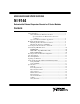
1 NI 9144 POWER FPGA RUN ERR Ether 2 4 INPUT 9-30 V 20 W MAX 1 2 LEDs IN Port 3 3 4 OUT Port Power Connector Figure 1. NI 9144 Chassis Safety Guidelines Operate the NI 9144 chassis only as described in this user guide. Safety Guidelines for Hazardous Locations The NI 9144 chassis is suitable for use in Class I, Division 2, Groups A, B, C, D, T4 hazardous locations; Class 1, Zone 2, AEx nA IIC T4 and Ex nA IIC T4 hazardous locations; and nonhazardous locations only.
Caution Substitution of components may impair suitability for Class I, Division 2. Caution For Zone 2 applications, install the system in an enclosure rated to at least IP 54 as defined by IEC 60529 and EN 60529. Special Conditions for Hazardous Locations Use in Europe This equipment has been evaluated as Ex nA IIC T4 equipment under DEMKO Certificate No. 07 ATEX 0626664X. Each chassis is marked II 3G and is suitable for use in Zone 2 hazardous locations, in ambient temperatures of –40 ≤ Ta ≤ 70 °C.
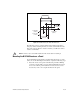
Cabling Clearance 50.8 mm (2.00 in.) 29.0 mm (1.14 in.) 48.4 mm (1.9 in.) 58.9 mm (2.32 in.) 286.4 mm (11.28 in.) 3.2 mm (0.13 in.) Figure 2. NI 9144 Chassis, Bottom View with Dimensions 165.1 mm (6.5 in.) 19.0 mm (0.75 in.) NI 9144 POWER FPGA RUN ERR 36.4 mm (1.43 in.) Ether 87.3 mm (3.44 in.) 51.7 mm (2.04 in.) INPUT 9-30 V 20 W MAX 2.9 mm (0.12 in.) Figure 3.
44.069 mm (1.74 in.) 25.078 mm (0.99 in.) 20.320 mm (0.8 in.) 44.125 mm (1.74 in.) 63.178 mm (2.49 in.) Figure 4. NI 9144 Chassis, Side View with Dimensions The following sections contain mounting method instructions. Before using any of these mounting methods, record the serial number from the back of the chassis. After the chassis is mounted, you will not be able to read the serial number. Caution Remove any C Series I/O modules from the chassis before mounting it.
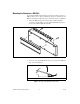
144 NI 9 er Eth UT INP V X A 9-30 WM 20 Figure 5. Installing the Panel Mount Accessory on the NI 9144 Chassis 330.200 mm (13 in.) 311.150 mm (12.25 in.) 286.634 mm (11.28 in.) 9.525 mm (0.38 in.) 15.491 mm (0.61 in.) NI 9144 POWER FPGA RUN ERR Ether 88.138 mm (3.47 in.) INPUT 9-30 V 20 W MAX 31.750 mm (1.25 in.) 63.500 mm (2.5 in.) Figure 6. Dimensions of NI 9144 Chassis with Panel Mount Accessory Installed 2.
Mounting the Chassis on a DIN Rail Use the NI 9915 DIN rail mount kit if you want to mount the chassis on a DIN rail. You need one clip for mounting the chassis on a standard 35 mm DIN rail. Complete the following steps to mount the chassis on a DIN rail: 1. Fasten the DIN rail clip to the chassis using a number 2 Phillips screwdriver and two M4 × 16 screws. National Instruments provides these screws with the DIN rail mount kit. Figure 7. Installing the DIN Rail Clip on the NI 9144 Chassis 2.
3. Press down firmly on the chassis to compress the spring until the clip locks in place on the DIN rail. Caution Remove any C Series I/O modules from the chassis before removing the chassis from the DIN rail. Connecting the NI 9144 Chassis to a Network NI recommends that you install a private network segment for your deterministic Ethernet expansion devices. Slave devices cause network flooding on a standard network.
Understanding LED Indications Figure 9 shows the NI 9144 chassis LEDs. POWER FPGA RUN ERR Figure 9. NI 9144 Chassis LEDs POWER LED The POWER LED is lit while the NI 9144 chassis is powered on. This LED indicates that the power supply connected to the chassis is adequate. FPGA LED—Open FPGA Mode Only This LED is for Open FPGA mode only. This mode is currently not activated. RUN and ERR LEDs The RUN LED is green and indicates that the NI 9144 is in an operational state.
Table 1.
Resetting the NI 9144 Network Configuration To reset the NI 9144 network configuration, unplug and replug in the NI 9144 chassis. Safe-State Outputs The NI 9144 has a safe state that lies between its configuration and operational states. When moving out of the operational state down to the configuration state, during normal operation or in case of a serious error, the NI 9144 passes through this safe state.
Using the NI 9144 with an EtherCAT Third-Party Master All of the functionality of the NI C Series modules is available to third-party masters using vendor extensions to the object dictionary. The NI 9144 is a modular device, meaning each module plugged into the backplane has its own object dictionary, and each module configuration is done through this dictionary. If your master software supports AoE services (ADS over EtherCAT), you can address the module directly.
Specifications The following specifications are typical for the –40 to 70°C operating temperature range unless otherwise noted. For more information, refer to the specific module specifications. Network Network interface ...................................100BaseTX Ethernet Compatibility ..........................................EtherCAT Communication rates ..............................100 Mbps Maximum cabling distance.....................
Measurement Category I is for measurements performed on circuits not directly connected to the electrical distribution system referred to as MAINS voltage. MAINS is a hazardous live electrical supply system that powers equipment. This category is for measurements of voltages from specially protected secondary circuits. Such voltage measurements include signal levels, special equipment, limited-energy parts of equipment, circuits powered by regulated low-voltage sources, and electronics.
Shock and Vibration To meet these specifications, you must panel mount the EtherCAT system and affix ferrules to the ends of the power terminal wires. Operating shock (IEC 60068-2-27) ........30 g, 11 ms half sine, 50 g, 3 ms half sine, 18 shocks at 6 orientations Operating vibration, random (IEC 60068-2-64) ......................5 grms, 10 to 500 Hz Operating vibration, sinusoidal (IEC 60068-2-6) ....................5 g, 10 to 500 Hz Cabling Table 2 shows the standard Ethernet cable wiring connections.
Connector 1 Pin 1 Connector 2 Pin 8 Pin 1 Pin 8 Figure 11. Ethernet Connector Pinout Safety Standards This product meets the requirements of the following standards of safety for electrical equipment for measurement, control, and laboratory use: • IEC 61010-1, EN 61010-1 • UL 61010-1, CSA 61010-1 Note For UL and other safety certifications, refer to the product label or the Online Product Certification section.
Note For EMC compliance, operate this device with shielded cables. CE Compliance This product meets the essential requirements of applicable European Directives as follows: • 2006/95/EC; Low-Voltage Directive (safety) • 2004/108/EC; Electromagnetic Compatibility Directive (EMC) Online Product Certification Refer to the product Declaration of Conformity (DoC) for additional regulatory compliance information. To obtain product certifications and the DoC for this product, visit ni.
Appendix A Vendor Extensions to the Object Dictionary Most object dictionary entries are defined by the relevant EtherCAT and CANOpen specification for modular slave devices. Both the NI 9144 device and the C Series modules have vendor extensions to the standard. These extensions are described here. Most object dictionary entries are set to usable defaults during the NI 9144’s transition from INIT to PREOP.
Table 3. Module Vendor Extensions (Continued) Index Sub Type R/W Description C Series Module Vendor Extensions 0x2000 0 U32 R 0x2001 0..
• NI 9422 • NI 9423 • NI 9425 • NI 9426 • NI 9435 • NI 9472 • NI 9474 • NI 9475 • NI 9477 • NI 9481 • NI 9485 NI 9201/9221 Table 4. NI 9201/9221 Vendor Configuration Extensions Index Sub Type R/W Description 0x2001 0 ARR:U32 — Scan List = 9 1 R Channels to Convert = 1..8, default = 8 2..
NI 9201/9221 Scan List The scan list channel codes consist of two bit fields in a 32-bit entry. Table 5. NI 9201/9221 Scan List Format Bits Field 31:24 =0 23:16 Data Offset[t] 15:8 =0 7:0 Convert Flag[t+2] Bits 23..16 describe the data offset to store a conversion at time t, and bits 7..0 describe the conversion control code that takes effect two conversions in the future, at time t+2.
NI 9201/9221 Calibration Data The NI 9201/9221 modules have eight channels with a nominal range of ±10.53 V and ±62.5 V, respectively. Each channel has an associated LSB weight, which is the number of volts per bit, and an offset, which is the number of volts per bit measured when the inputs are grounded. Note LSB weight is referred to as Gain in the object dictionary.
NI 9203 Table 8. NI 9203 Vendor Configuration Extensions Index Sub Type R/W Value 0x2001 0 ARR:U32 — Scan List = 9 1 R Channels to Convert = 1..8, default = 8 2..9 R/W Channel Code 0x2002 0 U32 R/W Unipolar Channel Mask 0x2100 0 ARR:U32 — Calibration = 36 1 R Bipolar Offset 2 R Ch0 Bipolar Gain 3 R Ch1 Gain ... — 9 R Ch7 Gain 10 R Unipolar Offset 11 R Ch0 Unipolar Gain ... — — 19 R R ... — External Calibration, Bipolar Gain ... ...
Table 9. NI 9203 Scan List Format (Continued) Bits Field 3 Bipolar = 0, Unipoloar = 1 2:0 Channel Code[t+2] Bits 23..16 describe the data offset to store a conversion at time t, and bits 3..0 describe the conversion control code that will take effect two conversions in the future, at time t+2. On the NI 9203, bit 3 determines whether the result is bipolar (signed) or unipolar (unsigned), and bits 2..0 are the channel number reversed. Table 10.
Table 11 contains the default scan list. Table 11. NI 9203 Scan List Format Index Sub Type Value 0x2001 0 ARR:U32 9 1 8 2 0x00000002 3 0x00010006 4 0x00020001 5 0x00030005 6 0x00040003 7 0x00050007 8 0x00060000 9 0x00070004 NI 9203 Calibration Data The NI 9203 has eight channels each with two modes. Each channel can have a nominal unipolar input range of 0–20 mA or bipolar ±20 mA.
The calibration data is stored in a U32 array, though each offset field should be interpreted as a signed value. Table 12. NI 9203 Calibration Coefficients Coefficient Representation Units LSB Weight Unsigned pA/LSB Offset Signed pA Use the calibration coefficients with the following equation to generate corrected data: ⎧ ⎨ ⎩ ∗ LSB weight – I offset ⎧ ⎪ ⎨ ⎪ ⎩ I raw – I expected 0mA ⎧ ⎪ ⎪ ⎪ ⎨ ⎪ ⎪ ⎪ ⎩ = ⎧ ⎪ ⎪ ⎨ ⎪ ⎪ ⎩ I corrected ( I raw ) pA bits pA/bit pA Table 13.
NI 9205/9206 Table 14. NI 9205/9206 Vendor Configuration Extensions Index Sub Type 0x2001 0 ARR:U32 0x2100 R/W Scan List = 33 1 R 2..33 R/W 0 ARR:U32 Description Channels to Convert = 1..32, default = 32 Channel Code — Calibration = 24 1 R Coeff 3 2 R Coeff 2 3 R Coeff 1 4 R Coeff 0 5 R 10 V offset 6 R 10 V gain 7 R 5 V offset ... — 13 R ...
Table 16. NI 9205/9206 Conversion Code Bits Field 15:13 001 = Read AI 12:11 Bank: 01 = Channels 0..15 10 = Channels 16..31 10:8 Channel LSB = 0..7 7:6 00 = Cal Pos Ref5V 5:4 00 = NRSE 11 = Cal Neg AI Gnd RSE or DIFF 3:2 Mode: 10 = Single–End A (Ch. 0..7, 16..23) 11 = Single–End B (Ch. 8..15, 24..
Table 17 contains the default scan list. Table 17.
3. Select the 32-bit offset value (to be interpreted as a signed int) for a particular range. 4. Use the above final coefficients and complete the following steps in the quadratic equation to convert raw 16-bit data into scaled volts: 5. a. a0 = (f64(a0) * rangeGain) + rangeOffset b. a1 = f64(a1) * rangeGain c. a2 = f64(a2) * rangeGain d. a3 = f64(a3) * rangeGain Use the following formula with a3–a0 to obtain the scaled 16-bit value in Volts.
Table 19 contains the default scan list. Table 19. NI 9211 Scan List Format Index Sub Type Value 0x2001 0 ARR:U32 7 1 6 2 0 3 1 ... ... 7 5 NI 9211 Calibration Data Calibration data is set up by the driver during initialization, and the calibration conversion is performed on the module ADC itself. NI 9213 Table 20. NI 9213 Vendor Configuration Extensions Index Sub Type R/W 0x2001 0 ARR:U32 — Scan List = 19 1 R Channels to Convert = 1..18, default = 18 2..
NI 9213 Conversion Speed Control The NI 9213 converts at two pre-defined rates, as controlled by the speed control field. Note The conversion rate assumes that 18 channels are in the scan list. Table 21. NI 9213 Conversion Speed Control Speed Control Meaning 2 (0x02) High-Accuracy 15 (0x0F) High-Speed Conversion 55 ms/channel (.99 s total) 740 μs/channel (13.32 ms total) NI 9213 Common Mode Error/Status The error/status field is shown in Table 22. Table 22.
Table 23 contains the default scan list. Table 23. NI 9213 Scan List Format Index Sub Type Value 0x2001 0 ARR:U32 19 1 18 2 0 3 1 ... ... 18 16 19 17 NI 9213 Calibration Data Calibration data is set up by the driver during initialization; the calibration conversion is performed on the module ADC. NI 9215 Table 24. NI 9215 Vendor Configuration Extensions Index Sub Type R/W 0x2100 0 ARR:U32 — Calibration = 16 1 R Ch0 Offset 2 R Ch0 Gain ... ...
NI 9215 Calibration Data The NI 9215 has four channels with a nominal range of ±10.4 V. Each channel has an associated LSB weight, which is the number of volts per bit, and an offset, which is the number of volts per bit measured when the inputs are grounded. Note LSB weight is referred to as Gain in the object dictionary. The NI 9215 EEPROM stores these two constants for each channel. The host can then take these constants and adjust the raw data into calibrated data.
Table 26. NI 9217 Vendor Configuration Extensions (Continued) Index Sub Type R/W Description 0x2100 0 ARR:U32 — Calibration = 16 1 R Ch0 Offset 2 R Ch0 Gain 3 R Ch1 Offset ... ... 8 R Ch3 Gain 9 R External Ch0 Offset ... ... ... ... NI 9217 Conversion Speed Control The NI 9217 converts at two pre-defined rates, as controlled by the speed control field. Note The conversion rate assumes that 4 channels are in the scan list. Table 27.
one conversion in the future, at time t+1. The conversion code is listed in Table 29. Table 29. NI 9217 Conversion Code Bits Field 7:3 Conversion rate: 0b11111 = 31, High-Accuracy 0b00010 = 2, High-Speed 2:1 Channel number 0 Reserved The conversion rate for every channel must match the value of the conversion speed control in 0x2002. Note For example, the scan list entry 0x00000001FC indicates this scan stores at address 1, and the next conversion is channel 2 at high-accuracy.
Note LSB weight is referred to as Gain in the object dictionary. The calibration data is stored in a U32 array, though each Offset field (subindex 1, 3, 5, and so on) should be interpreted as a signed value. Table 31.
Table 32. NI 9219 Vendor Configuration Extensions (Continued) Index Sub Type R/W 0x2100 0 ARR:U32 — Calibration = 168 1 R Ch0 60 V Offset 2 R Ch0 60 V Offset 3 R Ch0 15 V Offset ... ... 42 R Ch0 Full Bridge 7.8m V–V Gain 43 R Ch1 60 V Offset ... ... 0x2101 ... Description ... ... 0 ARR:U32 Q External Calibration = 168 1 — R Ch0 60 V Offset ... ... ... ...
NI 9219 Error Status Caution Configuring all the channels in full-bridge mode shorts the channels and results in the firmware setting all the bits in the lower nibble. When a channel over-current condition occurs on any of the channels of the NI 9219 (such as, configure channels in 4-wire resistance mode and do not connect a resistor to the channel), the firmware sets a bit in the lower nibble indicating the presence of this condition (LSB = ch0).
Table 34. NI 9219 Channel Calibration (Continued) Entry Number Mode 14 Range 3-Wire RTD Pt1000 15 Pt100 16 350 Ω Quarter-Bridge 120 Ω 17 18 Half-Bridge 19 Reserved 20 Full-Bridge ±500 mV/V — ±62.5 mV/V 21 ±7.8 mV/V The calibration data is stored in a U32 array, though each Offset field should be interpreted as a signed value. Table 35.
NI 9219 Configuration Commands There are eight configuration commands for the NI 9219. Eight configuration commands must be sent for each of the four channels. This is true even if you are only using a subset of the four channels. Each of the eight configuration commands is 1 Byte, each configuration command is followed by a data Byte, and then by a CRC value, which is 1 Byte. Hence, 3 Bytes * 8 Commands * 4 channels = 96 command bytes (held in 32 entries in the object dictionary).
NI 9219 Configuration Command Whether you are using the channel or not, you must configure the Conversion Time, Mode, Range, and Calibration Gain/Offset values for each channel on the NI 9219. You must first send calibration gain and offset values in MSB format. The Conversion Time value must be the same across all channels. Note Table 37. NI 9219 Scan List Format Bits Field 7:6 Channel Number, 0..3 5 =0 4:0 Configuration Type Where: Table 38.
NI 9219 Configuration Data Table 39. NI 9219 Type Conversion Time Configuration Value Max Frequency Conversion Time Description 0x01 100 Hz/50 Hz (TC) 10 ms/20 ms (TC) High Speed 0x08 9.09 Hz/8.33 Hz (TC) 110 ms/120 ms (TC) Best 60 Hz Rejection 0x09 7.69 Hz/7.14 Hz (TC) 130 ms/140 ms (TC) Best 50 Hz Rejection 0x0F 2 Hz/1.96 Hz (TC) 500 ms/510 ms (TC) High Resolution When any AI data channel is configured for Thermo-Couple, ADC conversion time increases by 10 ms for all channels.
Table 40. NI 9219 Mode and Range Type (Continued) Configuration Value (0x0F) Mode Range 350 Ω Quarter-Bridge 120 Ω (0x10) (0x11) Half-Bridge 1 V/V (0x13) Full-Bridge 62.5 mV/V (0x14) (0x17) 7.8 mV/V CJC CJC range NI 9219 Example Command Words Sequence Note The order in which you send the commands is important. Configuration 1: All Channels (ai0:ai3) for Voltage AI, ±15 Volt Range, High Speed Mode (100 Hz Max Sample Rate): Table 41.
Table 41.
Table 41.
Table 41.
Table 41. NI 9219 Configuration 1: Command Bytes (Continued) Command Byte Value Description 0x65 Data Byte 0xA0 CRC value NI 9233 As a DSA module, the NI 9233 does not synchronize to other modules and free-runs at its own fixed rate. Table 42. NI 9233 Vendor Configuration Extensions Index Sub Type R/W Description 0x2002 0 U32 R/W Configure ADC, default = 0x0A 0x2100 0 ARR:U32 — Calibration = 16 1 R Ch0 Offset 2 R Ch0 Gain 3 R Ch1 Offset ... ... ...
Where: Turbo Disable 0 The conversion rate is equal to the oversample clock rate/128. Set to 0 for conversion rates > 25 kS/s. 1 The conversion rate is equal to the oversample clock rate/256. Set to 1 for conversion rates < 25 kS/s. Clock Divisor The clock source (internal or external) is divided by this value and used as the converters’ oversample clock. Valid values are from 2 to 31, but the final divided clock must be between 512 kHz and 6.4 MHz.
Table 44. NI 9233 Calibration Data (Continued) Data Rate Turbo Disable Clock Divisor Clock Source Configure ADC Oversample Clock Rate 10.000 kS/s 1 00101 10 0x96 2.56 MHz 6.250 kS/s 1 01000 10 0xA2 1.60 MHz 5.000 kS/s 1 01010 10 0xAA 1.28 MHz 3.333 kS/s 1 01111 10 0xBE 853 kHz 3.125 kS/s 1 10000 10 0xC2 800 kHz 2.500 kS/s 1 10100 10 0xD2 640 kHz 2.000 kS/s 1 11001 10 0xE6 512 kHz NI 9233 Calibration Data The NI 9233 has four input channels with a fixed gain.
NI 9234 Table 46. NI 9234 Vendor Configuration Extensions Index Sub Type R/W Description 0x2002 0 U32 R/W 0x2100 0 ARR:U32 — Calibration = 16 1 R Ch0 Offset 2 R Ch0 Gain 3 R Ch0 Offset ... ... 8 R Ch3 Gain 9 R External Ch0 Offset ... ... Configure Module, default = 0x06 ... ... As a DSA module, the NI 9234 does not synchronize to other modules and free-runs at its own fixed rate. NI 9234 Configure Module The NI 9234 has a variety of configuration fields available.
Table 47. NI 9234 Scan List Format (Continued) Bits Field 6:2 Clock Divisor 1:0 Clock Source Where: IEPE Enable <3:0> When set, the corresponding channel’s relays are switched to IEPE operation. IEPE operations switches the AC/DC relay to AC mode and enables the IEPE relay to send the current to the IEPE sensor. AC/~DC <3:0> Controls the AC/DC relay when IEPE is not selected. If IEPE is enabled, then these bits have no meaning as AC mode is always selected with an IEPE operation.
NI 9234 Example Data Rates The example data rates use a 12.8 MHz clock source. Table 48. NI 9234 Example Data Rates Data Rate Clock Divisor Clock Source Rate Byte Oversample Clock Rate 50.000 kS/s 00001 10 0x06 12.80 MHz 25.000 kS/s 00010 10 0x0A 6.40 MHz 16.667 kS/s 00011 10 0x0E 4.27 MHz 12.500 kS/s 00100 10 0x12 3.20 MHz 10.000 kS/s 00101 10 0x16 2.56 MHz 6.250 kS/s 01000 10 0x22 1.60 MHz 5.000 kS/s 01010 10 0x2A 1.
NI 9237 Table 50. NI 9237 Vendor Configuration Extensions Index Sub Type R/W 0x2002 0 U32 R/W 0x2100 0 ARR:U16 Description Configure Module, default = 0x00060000 Calibration = 16 1 R Ch0 Offset 2 R Ch0 Gain 3 R Ch1 Offset ... ... ... 8 R Ch3 Gain 9 R External Ch0 Offset ... ... ... As a DSA module, the NI 9237 does not synchronize to other modules and free-runs at its own fixed rate.
Table 51. NI 9237 Scan List Format (Continued) Bits Field 6:4 Excitation 3:0 Offset Cal Enable Where: Shunt Cal Enable <3..0> Controls the shunt calibration switch for each of the four channels. A logic 1 in any bit closes the switch for the respective channel, while a logic 0 opens the switch. Half Bridge Enable <3..0> Controls the half bridge completion option for each channel.
Offset Cal Enable <3..0> Controls the offset calibration mode. Offset calibration mode disconnects both signal input pins and forces the channel inputs to zero volts, enabling measurement of the channel’s offset voltage. A logic 1 in any bit enables offset calibration for the respective channel, while a logic 0 disables it. Clock Divisor The NI 9237 divides the clock source (internal or external) by this value and uses it as the converters’ oversample clock.
NI 9237 Calibration Data The NI 9237 has four channels. Each channel has an associated LSB weight, which is the number of volts per bit, and an offset, which is the number of volts per bit measured when the inputs are grounded. Note LSB weight is referred to as Gain in the object dictionary. The calibration data is stored in a U16 array, though each Offset field (subindex 1, 3, 5, and so on) should be interpreted as a signed value. Table 53.
As a DSA module, the NI 9229/9239 does not synchronize to other modules and free-runs at its own fixed rate. For more information, refer to the NI 9233 Configure ADC section of this document. Note The NI 9229/9239 does not have the Turbo Bit configuration byte. NI 9229/9239 Calibration Data The NI 9229/9239 have four channels with nominal ranges of ±10 V and ±60 V respectively.
NI 9263 Table 56. NI 9263 Vendor Configuration Extensions Index Sub Type R/W Description 0x2100 0 ARR:U32 — Calibration = 16 1 R Ch0 Offset 2 R Ch0 Gain 3 R Ch1 Offset ... ... 8 R Ch3 Gain 9 R External Ch0 Offset ... ... NI 9263 Calibration Data The NI 9263 has four channels with a nominal range of ±10.7 V. Each channel has an associated LSB weight, which is the number of volts per bit, and an offset, which is the number of volts per bit measured when the inputs are grounded.
NI 9264 Table 58. NI 9264 Vendor Configuration Extensions Index Sub Type R/W Description 0x2100 1 ARR:U32 — Calibration = 16 2 R Ch0 Gain 3 R Ch1 Offset ... ... ... 8 R Ch3 Gain 9 R External Ch0 Offset ... ... ... NI 9264 Calibration Data The NI 9263 has four channels with a nominal range of ±10.5 V. Each channel has an associated LSB weight, which is the number of volts per bit, and an offset, which is the number of volts per bit measured when the inputs are grounded.
NI 9265 Table 60. NI 9265 Vendor Configuration Extensions Index Sub Type R/W Description 0x2002 1 ARR:U32 R Error Status, sent as 8-bit PDO 0x2100 0 ARR:U32 — Calibration = 16 1 R Ch0 Offset 2 R Ch0 Gain 3 R Ch1 Offset ... — 8 R Ch3 Gain 9 R External Ch0 Offset ... — NI 9265 Error Status Each channel has open loop detection circuitry that reports an error whenever the load is disconnected and the current is set to a value higher than 0 mA.
Use the calibration coefficients with the following equation to generate corrected data: pA – 12 A – 12 A I desired ( Code ) = Code • LSB weight ⎛ ---------⎞ • 10 ⎛ -------⎞ + Offset ( pA ) • 10 ⎛ -------⎞ ⎝ bits⎠ ⎝ pA⎠ ⎝ pA⎠ NI 9401 Table 62. NI 9401 Vendor Configuration Extensions Index Sub Type R/W Description 0x2001 0 U32 R/W Nibble direction control, default = 0 NI 9401 Direction Control Table 63.
NI 9403 Direction Control The direction control field has one bit for each I/O pin, with bit 0 matching channel 0, and so forth. 0 in the direction control indicates that I/O is an input; 1 indicates an output. Both the input and output data is transmitted in the PDO regardless of the direction control; only the relevant bits are connected to the I/O pins. Note NI 9476 Table 65.
Where to Go for Support The National Instruments Web site is your complete resource for technical support. At ni.com/support you have access to everything from troubleshooting and application development self-help resources to email and phone assistance from NI Application Engineers. National Instruments corporate headquarters is located at 11500 North Mopac Expressway, Austin, Texas, 78759-3504. National Instruments also has offices located around the world to help address your support needs.