
Single-Chip Microcontrollers User's Manual


256
CHAPTER 12 CLOCK OUTPUT CONTROL CIRCUIT
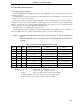
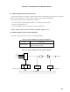
Remarks 1. fXX : Main system clock frequency (fX or fX/2)
2. fX : Main system clock oscillation frequency
3. f
XT : Subsystem clock oscillation frequency
4. TI00 : 16-bit timer/event counter input pin
5. TM0 : 16-bit timer register
6. MCS : Bit 0 of oscillation mode selection register (OSMS)
7. Figures in parentheses apply to operation with f
X = 5.0 MHz or fXT = 32.768 kHz.
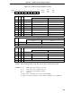
(2) Port mode register 3 (PM3)
This register set port 3 input/output in 1-bit units.
When using the P35/PCL pin for clock output function, set PM35 and output latch of P35 to 0.
PM3 is set with a 1-bit or 8-bit memory manipulation instruction.
RESET input sets PM3 to FFH.
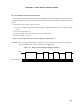
Figure 12-4. Port Mode Register 3 Format
PM37
7
PM36
6
PM35 PM34
4
PM33
3210
FF23H
Address
PM3
Symbol
PM32 PM31 PM30
5
FFH
After
Reset
R/W
R/W
PM3n
0
1
Output mode (output buffer ON)
Input mode (output buffer OFF)
P3n Pin Input/Output Mode Selection (n = 0 to 7)