
Datasheet


74AHC_AHCT1G66_4 © NXP B.V. 2008. All rights reserved.
Product data sheet Rev. 04 — 18 December 2008 10 of 17
NXP Semiconductors
74AHC1G66; 74AHCT1G66
Single-pole single-throw analog switch
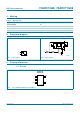
11.2 Additional dynamic characteristics
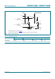
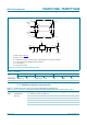
Test data is given in Table 11.
Definitions for test circuit:
R
T
= Termination resistance should be equal to output impedance Z
o
of the pulse generator.
C
L
= Load capacitance including jig and probe capacitance.
R
L
= Load resistance.
S1 = Test selection switch.
Fig 10. Test circuit for measuring switching times
V
M
V
M
t
W
t
W
10 %
90 %
0 V
V
I
V
I
negative
pulse
positive
pulse
0 V
V
M
V
M
90 %
10 %
t
f
t
r
t
r
t
f
001aad983
DUT
V
CC
V
CC
V
I
V
O
R
T
R
L
S1
C
L
open
G
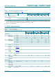
Table 11. Test data
Type Input Load S1 position
V
I
t
r
, t
f
C
L
R
L
t
PHL
, t
PLH
t
PZH
, t
PHZ
t
PZL
, t
PLZ
74AHC1G66 GND to V
CC
3 ns 15 pF, 50 pF 1 kΩ open GND V
CC
74AHCT1G66 GND to 3 V 3 ns 15 pF, 50 pF 1 kΩ open GND V
CC
Table 12. Additional dynamic characteristics for 74AHC1G66 and 74AHCT1G66
GND = 0 V; t
r
= t
f
= 3.0 ns; C
L
= 50 pF; unless otherwise specified. All typical values are measured at T
amb
=25
°
C.
Symbol Parameter Conditions Min Typ Max Unit
THD total harmonic
distortion
f
i
= 1 kHz; R
L
= 10 kΩ; see Figure 11
V
CC
= 3.0 V to 3.6 V - 0.025 - %
V
CC
= 4.5 V to 5.5 V - 0.015 - %
f
i
= 10 kHz; R
L
= 10 kΩ; see Figure 11
V
CC
= 3.0 V to 3.6 V; V
I
= 2.5 V - 0.025 - %
V
CC
= 4.5 V to 5.5 V; V
I
= 4.0 V - 0.015 - %