
Datasheet


74AHC_AHCT1G66_4 © NXP B.V. 2008. All rights reserved.
Product data sheet Rev. 04 — 18 December 2008 11 of 17
NXP Semiconductors
74AHC1G66; 74AHCT1G66
Single-pole single-throw analog switch
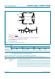
[1] Adjust input voltage V
I
to 0 dBm level (0 dBm =1 mW into 50 Ω).
11.3 Test circuits and graphs
f
(−3dB)
−3 dB frequency
response
R
L
= 50 Ω; C
L
=10pF;
see
Figure 12 and 13
V
CC
= 3.0 V to 3.6 V - 230 - MHz
V
CC
= 4.5 V to 5.5 V - 280 - MHz
α
iso
isolation (OFF-state) R
L
= 600 Ω; f
i
= 1 MHz; see Figure 14
[1]
V
CC
= 3.0 V to 3.6 V; V
I
= 2.5 V - −50 - dB
V
CC
= 4.5 V to 5.5 V; V
I
= 4.0 V - −50 - dB
Table 12. Additional dynamic characteristics for 74AHC1G66 and 74AHCT1G66
…continued
GND = 0 V; t
r
= t
f
= 3.0 ns; C
L
= 50 pF; unless otherwise specified. All typical values are measured at T
amb
=25
°
C.
Symbol Parameter Conditions Min Typ Max Unit
Test conditions:
V
CC
= 3.0 V to 3.6 V; V
I
= 2.5 V (p-p).
V
CC
= 4.5 V to 5.5 V; V
I
= 4.0 V (p-p).
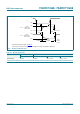
Fig 11. Test circuit for measuring total harmonic distortion
10 µF
2R
L
2R
L
C
L
f
i
V
IH
V
O
V
CC
V
CC
E
D
Y/Z Z/Y
001aai678
With f
i
= 1 MHz adjust the switch input voltage for a 0 dBm level at the switch output, (0 dBm = 1 mW into 50 Ω). Then increase
the input f
i
frequency until the dB meter reads −3dB.
Fig 12. Test circuit for measuring the −3 dB frequency response
0.1 µF
2R
L
2R
L
C
L
f
i
V
IH
V
O
V
CC
V
CC
E
dB
Y/Z Z/Y
001aai680