
Datasheet


74AHC_AHCT1G66_4 © NXP B.V. 2008. All rights reserved.
Product data sheet Rev. 04 — 18 December 2008 3 of 17
NXP Semiconductors
74AHC1G66; 74AHCT1G66
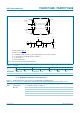
Single-pole single-throw analog switch
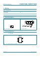
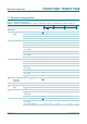
6.2 Pin description
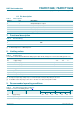
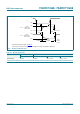
7. Functional description
[1] H = HIGH voltage level; L = LOW voltage level.
8. Limiting values
[1] The input and output voltage ratings may be exceeded if the input and output voltage ratings are observed.
[2] For TSSOP5 and SC-74A packages: above 87.5 °C the value of P
tot
derates linearly with 4.0 mW/K.
9. Recommended operating conditions
Table 3. Pin description
Symbol Pin Description
Y 1 independent input or output
Z 2 independent input or output
GND 3 ground (0 V)
E 4 enable input (active HIGH)
V
CC
5 supply voltage
Table 4. Function table
[1]
Input E Switch
L OFF
HON
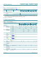
Table 5. Limiting values
In accordance with the Absolute Maximum Rating System (IEC 60134). Voltages are referenced to GND (ground = 0 V).
Symbol Parameter Conditions Min Max Unit
V
CC
supply voltage −0.5 +7.0 V
I
IK
input clamping current V
I
< −0.5 V
[1]
−20 - mA
I
SK
switch clamping current V
I
< −0.5 V or V
I
>V
CC
+ 0.5 V
[1]
- ±20 mA
I
SW
switch current −0.5 V < V
O
< V
CC
+ 0.5 V - ±25 mA
I
CC
supply current - 75 mA
I
GND
ground current −75 - mA
T
stg
storage temperature −65 +150 °C
P
tot
total power dissipation T
amb
= −40 °C to +125 °C
[2]
- 250 mW
Table 6. Recommended operating conditions
Voltages are referenced to GND (ground = 0 V).
[1]
Symbol Parameter Conditions 74AHC1G66 74AHCT1G66 Unit
Min Typ Max Min Typ Max
V
CC
supply voltage 2.0 5.0 5.5 4.5 5.0 5.5 V
V
I
input voltage 0 - 5.5 0 - 5.5 V
V
SW
switch voltage 0 - V
CC
0-V
CC
V