
Datasheet


74AHC_AHCT1G66_4 © NXP B.V. 2008. All rights reserved.
Product data sheet Rev. 04 — 18 December 2008 8 of 17
NXP Semiconductors
74AHC1G66; 74AHCT1G66
Single-pole single-throw analog switch
[1] All typical values are measured at V
CC
= 2.0 V, V
CC
= 3.3 V, V
CC
= 5.0 V and T
amb
=25°C.
[2] t
pd
is the same as t
PLH
and t
PHL
.
t
en
is the same as t
PZL
and t
PZH
.
t
dis
is the same as t
PLZ
and t
PHZ
.
[3] C
PD
is used to determine the dynamic power dissipation P
D
(µW).
P
D
=C
PD
× V
CC
2
× f
i
+ Σ ((C
L
× C
SW
) × V
CC
2
× f
o
) where:
f
i
= input frequency in MHz;
f
o
= output frequency in MHz;
C
L
= output load capacitance in pF;
C
SW
= maximum switch capacitance in pF (see Table 7);
V
CC
= supply voltage in Volt;
Σ ((C
L
× C
SW
) × V
CC
2
× f
o
) = sum of outputs.
11.1 Waveforms and test circuit
C
PD
power
dissipation
capacitance
V
I
= GND to V
CC
[3]
15 - - - pF
Table 9. Dynamic characteristics
…continued
Voltages are referenced to GND (ground = 0 V);
C
L
= 50 pF; unless otherwise specified;
For test circuit see Figure 10.
Symbol Parameter Conditions 25 °C −40 °C to +85 °C −40 °C to +125 °C Unit
Typ
[1]
max Max Max
Measurement points are given in Table 10.
Logic levels: V
OL
and V
OH
are typical output voltage levels that occur with the output load.
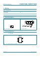
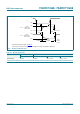
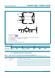
Fig 8. Input (Y or Z) to output (Z or Y) propagation delays
mna667
t
PLH
t
PHL
V
M
V
M
Y or Z input
Z or Y output
GND
V
I
V
OH
V
OL