
Datasheet

74HC_HCT2G66 All information provided in this document is subject to legal disclaimers. © NXP B.V. 2013. All rights reserved.
Product data sheet Rev. 10 — 3 October 2013 4 of 23
NXP Semiconductors 74HC2G66; 74HCT2G66
Dual single-pole single-throw analog switch
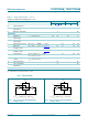
7. Functional description
[1] H = HIGH voltage level; L = LOW voltage level.
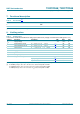
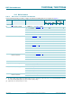
8. Limiting values
[1] The input and output voltage ratings may be exceeded if the input and output current ratings are observed.
[2] For TSSOP8 packages: above 55 C the value of P
tot
derates linearly with 2.5 mW/K.
For VSSOP8 packages: above 110 C the value of P
tot
derates linearly with 8.0 mW/K.
For XSON8 packages: above 118 C the value of P
tot
derates linearly with 7.8 mW/K.
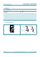
Table 4. Function table
[1]
Input nE Switch
LOFF
HON
Table 5. Limiting values
In accordance with the Absolute Maximum Rating System (IEC 60134). Voltages are referenced to GND (ground = 0 V).
Symbol Parameter Conditions Min Max Unit
V
CC
supply voltage 0.5 +11.0 V
I
IK
input clamping current V
I
< 0.5 V or V
I
>V
CC
+ 0.5 V
[1]
- 20 mA
I
SK
switch clamping current V
I
< 0.5 V or V
I
>V
CC
+ 0.5 V
[1]
- 20 mA
I
SW
switch current V
SW
> 0.5 V or V
SW
< V
CC
+ 0.5 V - 20 mA
I
CC
supply current - 30 mA
I
GND
ground current 30 - mA
T
stg
storage temperature 65 +150 C
P
tot
total power dissipation T
amb
= 40 C to +125 C
per package
[2]
- 300 mW
per switch
[2]
- 100 mW