
Datasheet

74HC_HCT2G66 All information provided in this document is subject to legal disclaimers. © NXP B.V. 2013. All rights reserved.
Product data sheet Rev. 10 — 3 October 2013 9 of 23
NXP Semiconductors 74HC2G66; 74HCT2G66
Dual single-pole single-throw analog switch
[1] All typical values are measured at T
amb
=25C.
[2] t
pd
is the same as t
PLH
and t
PHL
.
t
en
is the same as t
PZL
and t
PZH
.
t
dis
is the same as t
PLZ
and t
PHZ
.
[3] C
PD
is used to determine the dynamic power dissipation P
D
(W).
P
D
=C
PD
V
CC
2
f
i
+ ((C
L
C
SW
) V
CC
2
f
o
)where:
f
i
= input frequency in MHz;
f
o
= output frequency in MHz;
C
L
= output load capacitance in pF;
C
SW
= maximum switch capacitance in pF (see Table 7);
V
CC
= supply voltage in volts;
((C
L
C
SW
) V
CC
2
f
o
) = sum of outputs.
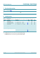
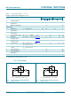
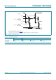
11.1 Waveforms and test circuit
74HCT2G66
t
pd
propagation delay nY to nZ or nZ to nY; R
L
= ;
see Figure 10
[2]
V
CC
= 4.5 V - 2 15 - 18 ns
t
en
enable time nE to nY or nZ; see Figure 11
[2]
V
CC
= 4.5 V - 13 30 - 36 ns
t
dis
disable time nE to nY or nZ; see Figure 11
[2]
V
CC
= 4.5 V - 13 44 - 53 ns
C
PD
power dissipation
capacitance
V
I
=GNDtoV
CC
1.5 V
[3]
-9-- -pF
Table 9. Dynamic characteristics
…continued
Voltages are referenced to GND (ground = 0 V); For test circuit see Figure 12.
Symbol Parameter Conditions 40 C to +85 C 40 C to +125 C Unit
Min Typ
[1]
Max Min Max
Measurement points are given in Table 10.
Logic levels: V
OL
and V
OH
are typical output voltage levels that occur with the output load.
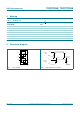
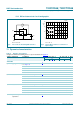
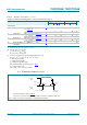
Fig 10. Input (nY or nZ) to output (nZ or nY) propagation delays
001aaa541
t
PLH
t
PHL
V
M
V
M
V
M
V
M
nY or nZ
input
nZ or nY
output
GND
V
I
V
OH
V
OL