
Datasheet

74HC_HCT4052 All information provided in this document is subject to legal disclaimers. © NXP B.V. 2012. All rights reserved.
Product data sheet Rev. 10 — 19 July 2012 5 of 29
NXP Semiconductors
74HC4052; 74HCT4052
Dual 4-channel analog multiplexer/demultiplexer
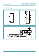
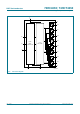
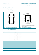
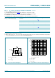
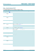
6. Pinning information
6.1 Pinning
6.2 Pin description
(1) The die substrate is attached to this pad using
conductive die attach material. It can not be used as
supply pin or input.
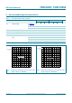
Fig 5. Pin configuration for DIP16, SO16 and
(T)SSOP16
Fig 6. Pin configuration for DHVQFN16
74HC4052
74HCT4052
2Y0 V
CC
2Y2 1Y2
2Z 1Y1
2Y3 1Z
2Y1 1Y0
E 1Y3
V
EE
S0
GND S1
001aah822
1
2
3
4
5
6
7
8
10
9
12
11
14
13
16
15
001aah823
74HC4052
74HCT4052
V
EE
V
CC
(1)
S0
E 1Y3
2Y1 1Y0
2Y3 1Z
2Z 1Y1
2Y2 1Y2
GND
S1
2Y0
V
CC
Transparent top view
7 10
6 11
5 12
4
13
3 14
2 15
8
9
1
16
terminal 1
index area
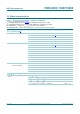
Table 2. Pin description
Symbol Pin Description
2Y0 1 independent input or output 2Y0
2Y2 2 independent input or output 2Y2
2Z 3 common input or output 2
2Y3 4 independent input or output 2Y3
2Y1 5 independent input or output 2Y1
E
6 enable input (active LOW)
V
EE
7 negative supply voltage
GND 8 ground (0 V)
S1 9 select logic input 1
S0 10 select logic input 0
1Y3 11 independent input or output 1Y3
1Y0 12 independent input or output 1Y0
1Z 13 common input or output 1
1Y1 14 independent input or output 1Y1
1Y2 15 independent input or output 1Y2
V
CC
16 positive supply voltage