
Datasheet

74HC_HCT4052 All information provided in this document is subject to legal disclaimers. © NXP B.V. 2012. All rights reserved.
Product data sheet Rev. 10 — 19 July 2012 6 of 29
NXP Semiconductors
74HC4052; 74HCT4052
Dual 4-channel analog multiplexer/demultiplexer
7. Functional description
7.1 Function table
[1] H = HIGH voltage level;
L = LOW voltage level;
X = don’t care.
8. Limiting values
[1] To avoid drawing V
CC
current out of pins nZ, when switch current flows in pins nYn, the voltage drop across the bidirectional switch must
not exceed 0.4 V. If the switch current flows into pins nZ, no V
CC
current will flow out of pins nYn. In this case there is no limit for the
voltage drop across the switch, but the voltages at pins nYn and nZ may not exceed V
CC
or V
EE
.
[2] For DIP16 packages: above 70 C the value of P
tot
derates linearly with 12 mW/K.
[3] For SO16 packages: above 70 C the value of P
tot
derates linearly with 8 mW/K.
For SSOP16 and TSSOP16 packages: above 60 C the value of P
tot
derates linearly with 5.5 mW/K.
For DHVQFN16 packages: above 60 C the value of P
tot
derates linearly with 4.5 mW/K.
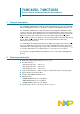
Table 3. Function table
[1]
Input Channel on
E S1 S0
LLLnY0 and nZ
L L H nY1 and nZ
LHLnY2 and nZ
L HHnY3 and nZ
H X X none
Table 4. Limiting values
In accordance with the Absolute Maximum Rating System (IEC 60134).
Voltages are referenced to V
EE
= GND (ground = 0 V).
Symbol Parameter Conditions Min Max Unit
V
CC
supply voltage
[1]
0.5 +11.0 V
I
IK
input clamping current V
I
< 0.5 V or V
I
>V
CC
+0.5V - 20 mA
I
SK
switch clamping current V
SW
< 0.5 V or V
SW
>V
CC
+0.5V - 20 mA
I
SW
switch current 0.5 V < V
SW
<V
CC
+0.5V - 25 mA
I
EE
supply current - 20 mA
I
CC
supply current - 50 mA
I
GND
ground current - 50 mA
T
stg
storage temperature 65 +150 C
P
tot
total power dissipation DIP16 package
[2]
- 750 mW
SO16, (T)SSOP16, and DHVQFN16
package
[3]
- 500 mW
P power dissipation per switch - 100 mW