
Datasheet

74HC_HCT4052 All information provided in this document is subject to legal disclaimers. © NXP B.V. 2012. All rights reserved.
Product data sheet Rev. 10 — 19 July 2012 7 of 29
NXP Semiconductors
74HC4052; 74HCT4052
Dual 4-channel analog multiplexer/demultiplexer
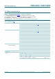
9. Recommended operating conditions
Table 5. Recommended operating conditions
Symbol Parameter Conditions 74HC4052 74HCT4052 Unit
Min Typ Max Min Typ Max
V
CC
supply voltage see Figure 7
and Figure 8
V
CC
GND 2.0 5.0 10.0 4.5 5.0 5.5 V
V
CC
V
EE
2.0 5.0 10.0 2.0 5.0 10.0 V
V
I
input voltage GND - V
CC
GND - V
CC
V
V
SW
switch voltage V
EE
-V
CC
V
EE
-V
CC
V
T
amb
ambient temperature 40 +25 +125 40 +25 +125 C
t/V input transition rise and fall
rate
V
CC
= 2.0 V - - 625 - - - ns/V
V
CC
= 4.5 V - 1.67 139 - 1.67 139 ns/V
V
CC
=6.0V - - 83 - - - ns/V
V
CC
= 10.0 V - - 31 - - - ns/V
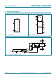
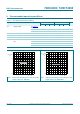
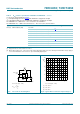
Fig 7. Guaranteed operating area as a function of the
supply voltages for 74HC4052
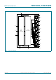
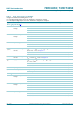
Fig 8. Guaranteed operating area as a function of the
supply voltages for 74HCT4052
mnb044
04 12
12
0
4
8
8
operating area
V
CC
− V
EE
(V)
V
CC
− GND
(V)
mnb045
0
12
6
10
8
2
4
04 128
operating area
V
CC
− V
EE
(V)
V
CC
− GND
(V)