
Datasheet

74HC_HCT4052 All information provided in this document is subject to legal disclaimers. © NXP B.V. 2012. All rights reserved.
Product data sheet Rev. 10 — 19 July 2012 9 of 29
NXP Semiconductors
74HC4052; 74HCT4052
Dual 4-channel analog multiplexer/demultiplexer
[1] All typical values are measured at T
amb
=25C.
[2] When supply voltages (V
CC
V
EE
) near 2.0 V the analog switch ON resistance becomes extremely non-linear. When using a supply of
2 V, it is recommended to use these devices only for transmitting digital signals.
R
ON(rail)
ON resistance (rail) V
is
=V
EE
V
CC
= 2.0 V; V
EE
= 0 V; I
SW
= 100 A
[2]
---
V
CC
= 4.5 V; V
EE
= 0 V; I
SW
= 1000 A --210
V
CC
= 6.0 V; V
EE
= 0 V; I
SW
= 1000 A --180
V
CC
= 4.5 V; V
EE
= 4.5 V; I
SW
= 1000 A --160
V
is
=V
CC
V
CC
= 2.0 V; V
EE
= 0 V; I
SW
= 100 A
[2]
---
V
CC
= 4.5 V; V
EE
= 0 V; I
SW
= 1000 A --240
V
CC
= 6.0 V; V
EE
= 0 V; I
SW
= 1000 A --210
V
CC
= 4.5 V; V
EE
= 4.5 V; I
SW
= 1000 A --180
Table 6. R
ON
resistance per switch for 74HC4052 and 74HCT4052 …continued
V
I
= V
IH
or V
IL
; for test circuit see Figure 9.
V
is
is the input voltage at a nYn or nZ terminal, whichever is assigned as an input.
V
os
is the output voltage at a nYn or nZ terminal, whichever is assigned as an output.
For 74HC4052: V
CC
GND or V
CC
V
EE
= 2.0 V, 4.5 V, 6.0 V and 9.0 V.
For 74HCT4052: V
CC
GND = 4.5 V and 5.5 V, V
CC
V
EE
= 2.0 V, 4.5 V, 6.0 V and 9.0 V.
Symbol Parameter Conditions Min Typ Max Unit
V
is
=0Vto(V
CC
V
EE
). V
is
=0Vto(V
CC
V
EE
).
(1) V
CC
=4.5V
(2) V
CC
=6V
(3) V
CC
=9V
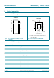
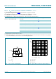
Fig 9. Test circuit for measuring R
ON
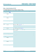
Fig 10. Typical R
ON
as a function of input voltage V
is
V
001aah826
nYn
Snfrom select
input
nZ
GND V
EE
V
CC
V
is
I
sw
V
sw
V
is
(V)
0 9.07.23.6 5.41.8
001aai068
40
60
20
80
100
R
ON
(Ω)
0
(1)
(2)
(3)
R
ON
V
sw
I
sw
---------
=