
Datasheet


74HC_HCT4053 All information provided in this document is subject to legal disclaimers. © NXP B.V. 2012. All rights reserved.
Product data sheet Rev. 8 — 19 July 2012 4 of 32
NXP Semiconductors
74HC4053; 74HCT4053
Triple 2-channel analog multiplexer/demultiplexer
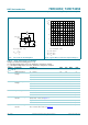
6. Pinning information
6.1 Pinning
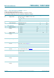
Fig 4. Schematic diagram (one switch)
001aad544
from
logic
V
CC
V
EE
V
EE
V
CC
V
CC
V
EE
Y
Z
V
CC
(1) This is not a supply pin. The substrate is attached to this
pad using conductive die attach material. There is no
electrical or mechanical requirement to solder this pad.
However, if it is soldered, the solder land should remain
floating or be connected to V
CC
.
Fig 5. Pin configuration DIP16, SO16, and (T)SSOP16 Fig 6. Pin configuration DHVQFN16
74HC4053
74HCT4053
2Y1 V
CC
2Y0 2Z
3Y1 1Z
3Z 1Y1
3Y0 1Y0
ES1
V
EE
S2
GND S3
001aae127
1
2
3
4
5
6
7
8
10
9
12
11
14
13
16
15
001aae128
V
EE
S2
ES1
3Y0 1Y0
3Z 1Y1
3Y1 1Z
2Y0 2Z
GND
S3
2Y1
V
CC
Transparent top view
7 10
6 11
5 12
4
13
3 14
2 15
8
9
1
16
terminal 1
index area
V
CC
(1)
74HC4053
74HCT4053