INTEGRATED CIRCUITS DATA SHEET For a complete data sheet, please also download: • The IC06 74HC/HCT/HCU/HCMOS Logic Family Specifications • The IC06 74HC/HCT/HCU/HCMOS Logic Package Information • The IC06 74HC/HCT/HCU/HCMOS Logic Package Outlines 74HC/HCT4511 BCD to 7-segment latch/decoder/driver Product specification File under Integrated Circuits, IC06 December 1990
Philips Semiconductors Product specification BCD to 7-segment latch/decoder/driver 74HC/HCT4511 ripple blanking input (BI), an active LOW lamp test input (LT), and seven active HIGH segment outputs (Qa to Qg). FEATURES • Latch storage of BCD inputs When LE is LOW, the state of the segment outputs (Qa to Qg) is determined by the data on D1 to D4. When LE goes HIGH, the last data present on D1 to D4 are stored in the latches and the segment outputs remain stable.
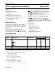
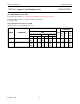
Philips Semiconductors Product specification BCD to 7-segment latch/decoder/driver 74HC/HCT4511 ORDERING INFORMATION See “74HC/HCT/HCU/HCMOS Logic Package Information”. PIN DESCRIPTION PIN NO. SYMBOL NAME AND FUNCTION 3 LT lamp test input (active LOW) 4 BI ripple blanking input (active LOW) 5 LE latch enable input (active LOW) 7, 1, 2, 6 D1 to D4 BCD address inputs 8 GND ground (0 V) 13, 12, 11, 10, 9, 15, 14 Qa to Qg segments outputs 16 VCC positive supply voltage Fig.
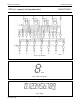
Philips Semiconductors Product specification BCD to 7-segment latch/decoder/driver 74HC/HCT4511 Fig.4 Functional diagram.
Philips Semiconductors Product specification BCD to 7-segment latch/decoder/driver Fig.5 Logic diagram. Fig.6 Segment designation. Fig.7 Display.
Philips Semiconductors Product specification BCD to 7-segment latch/decoder/driver 74HC/HCT4511 DC CHARACTERISTICS FOR 74HC For the DC characteristics see “74HC/HCT/HCU/HCMOS Logic Family Specifications”. Output capability: standard, excepting VOH which is given below ICC category: MSI Non-standard DC characteristics for 74HC Voltages are referenced to GND (ground = 0 V) Tamb (°C) SYMBOL TEST CONDITIONS 74HC PARAMETER +25 min. typ. −40 to +85 UNIT VCC (V) −40 to +125 VI −IO (mA) max. min. max.
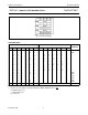
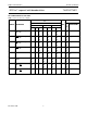
Philips Semiconductors Product specification BCD to 7-segment latch/decoder/driver 74HC/HCT4511 AC CHARACTERISTICS FOR 74HC GND = 0 V; tr = tf = 6 ns; CL = 50 pF Tamb (°C) TEST CONDITIONS 74HC SYMBOL PARAMETER +25 min. typ. −40 to +85 max. min. max. −40 to +125 min. UNIT VCC WAVEFORMS (V) max. tPHL/ tPLH propagation delay Dn to Qn 77 28 22 300 60 51 375 75 64 450 90 77 ns 2.0 4.5 6.0 Fig.8 tPHL/ tPLH propagation delay LE to Qn 74 27 22 270 54 46 330 68 58 405 81 69 ns 2.0 4.
Philips Semiconductors Product specification BCD to 7-segment latch/decoder/driver 74HC/HCT4511 DC CHARACTERISTICS FOR 74HCT For the DC characteristics see “74HC/HCT/HCU/HCMOS Logic Family Specifications”. Output capability: standard, excepting VOH which is given below ICC category: MSI Non-standard DC characteristics for 74HCT Voltages are referenced to GND (ground = 0 V) Tamb (°C) SYMBOL 74HCT PARAMETER +25 min. VOH HIGH level output voltage TEST CONDITIONS typ.
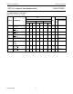
Philips Semiconductors Product specification BCD to 7-segment latch/decoder/driver 74HC/HCT4511 AC CHARACTERISTICS FOR 74HCT GND = 0 V; tr = tf = 6 ns; CL = 50 pF Tamb (°C) TEST CONDITIONS 74HCT SYMBOL PARAMETER +25 min. −40 to +85 typ. max. min. max. −40 to +125 min. UNIT VCC (V) WAVEFORMS max. tPHL/ tPLH propagation delay Dn to Qn 28 60 75 90 ns 4.5 Fig.8 tPHL/ tPLH propagation delay LE to Qn 27 54 68 81 ns 4.5 Fig.
Philips Semiconductors Product specification BCD to 7-segment latch/decoder/driver 74HC/HCT4511 AC WAVEFORMS (1) HC : VM = 50%; VI = GND to VCC. HCT: VM = 1.3 V; VI = GND to 3 V. (1) HC : VM = 50%; VI = GND to VCC. HCT: VM = 1.3 V; VI = GND to 3 V. Fig.8 Fig.9 Waveforms showing the input (Dn, LT) to output (Qn) propagation delays and the output transition times. Waveforms showing the input (LE) to output (Qn) propagation delays and the latch enable pulse width.
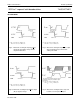
Philips Semiconductors Product specification BCD to 7-segment latch/decoder/driver 74HC/HCT4511 APPLICATION DIAGRAMS Fig.13 Connection to common anode LED display readout. Fig.12 Connection to common cathode LED display readout. (1) A filament pre-warm resistor to reduce thermal shock and to increase effective cold resistance of the filament is recommended. Fig.14 Connection to incandescent display readout. Fig.15 Connection to fluorescent display readout. Fig.
Philips Semiconductors Product specification BCD to 7-segment latch/decoder/driver PACKAGE OUTLINES See “74HC/HCT/HCU/HCMOS Logic Package Outlines”.