
Datasheet


September 1993 3
Philips Semiconductors Product specification
Programmable delay timer with oscillator 74HC/HCT5555
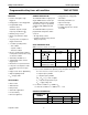
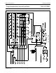
PINNING
SYMBOL PIN DESCRIPTION
RS 1 clock input/oscillator pin
R
TC
2 external resistor connection
C
TC
3 external capacitor connection
A 4 trigger input (positive-edge
triggered)
B 5 trigger input (negative-edge
triggered)
RTR/
RTR 6 retriggerable/non-retriggerable
input (active HIGH/active LOW)
Q 7 pulse output (active LOW)
GND 8 ground (0 V)
Q 9 pulse output (active HIGH)
S
0
− S
3
10, 11,
12, 13
programmable input
OSC CON 14 oscillator control
MR 15 master reset input (active
HIGH)
V
CC
16 positive supply voltage
Fig.1 Pin configuration.
handbook, halfpage
1
2
3
4
5
6
7
8
16
15
14
13
12
11
10
9
5555
GND
V
CC
MGA642
R
TC
C
TC
Q
RS
OSC
CON
MR
A
B
RTR/
RTR
Q
0
S
1
S
2
S
S
3
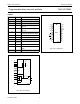
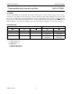
Fig.2 IEC logic diagram.
handbook, halfpage
MGA643
1
I = 0
S
R
R
&
CT = 0
CT = m R
V16
7
9
17
16G17
CX
RX
1
2
4
8
X / Y CTRDIVm
[T]
Y = 0
Y = 15
! G
+
0
15
10
11
12
13
2
3
14
1
6
4
5
15