
Datasheet

xxxxxxxxxxxxxxxxxxxxx xxxxxxxxxxxxxxxxxxxxxxxxxx xxxxxxx x x x xxxxxxxxxxxxxxxxxxxxxxxxxxxxxx xxxxxxxxxxxxxxxxxxx xx xx xxxxx
xxxxxxxxxxxxxxxxxxxxxxxxxxx xxxxxxxxxxxxxxxxxxx xxxxxx xxxxxxxxxxxxxxxxxxxxxxxxxxxxxxxxxxx xxxxxxxxxxxx x x
xxxxxxxxxxxxxxxxxxxxx xxxxxxxxxxxxxxxxxxxxxxxxxxxxxx xxxxx xxxxxxxxxxxxxxxxxxxxxxxxxxxxxxxxxxxxxxxxxxxxxxxxxx xxxxxxxx
xxxxxxxxxxxxxxxxxxxxxxxxx xxxxxxxxxxxxxxxxxxxx xxx
ADC1015S_SER All information provided in this document is subject to legal disclaimers. © NXP B.V. 2010. All rights reserved.
Product data sheet Rev. 2 — 20 December 2010 11 of 42
NXP Semiconductors
ADC1015S series
Single 10-bit ADC; input buffer; CMOS or LVDS DDR digital outputs
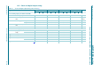
[1] Typical values measured at V
DDA(3V)
=3V, V
DDO
= 1.8 V, V
DDA(5V)
=5V; T
amb
=25C and C
L
= 5 pF; minimum and maximum values are across the full temperature range
T
amb
= 40 C to +85 C at V
DDA(3V)
=3V, V
DDO
=1.8V, V
DDA(5V)
=5V, V
INP
V
INM
= 1 dBFS; internal reference mode; applied to CMOS and LVDS interface; unless otherwise
specified.
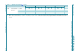
IMD Intermodulation
distortion
f
i
=3MHz -89--89--92--93-dBc
f
i
=30MHz-88--88--92--92-dBc
f
i
=70MHz-87--87--90--90-dBc
f
i
=170MHz-84--85--87--88-dBc
Table 7. Dynamic characteristics
[1]
…continued
Symbol Parameter Conditions ADC1015S065 ADC1015S080 ADC1015S105 ADC1015S125 Unit
Min Typ Max Min Typ Max Min Typ Max Min Typ Max