
Datasheet

xxxxxxxxxxxxxxxxxxxxx xxxxxxxxxxxxxxxxxxxxxxxxxx xxxxxxx x x x xxxxxxxxxxxxxxxxxxxxxxxxxxxxxx xxxxxxxxxxxxxxxxxxx xx xx xxxxx
xxxxxxxxxxxxxxxxxxxxxxxxxxx xxxxxxxxxxxxxxxxxxx xxxxxx xxxxxxxxxxxxxxxxxxxxxxxxxxxxxxxxxxx xxxxxxxxxxxx x x
xxxxxxxxxxxxxxxxxxxxx xxxxxxxxxxxxxxxxxxxxxxxxxxxxxx xxxxx xxxxxxxxxxxxxxxxxxxxxxxxxxxxxxxxxxxxxxxxxxxxxxxxxx xxxxxxxx
xxxxxxxxxxxxxxxxxxxxxxxxx xxxxxxxxxxxxxxxxxxxx xxx
ADC1015S_SER All information provided in this document is subject to legal disclaimers. © NXP B.V. 2010. All rights reserved.
Product data sheet Rev. 2 — 20 December 2010 12 of 42
NXP Semiconductors
ADC1015S series
Single 10-bit ADC; input buffer; CMOS or LVDS DDR digital outputs
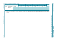
10.2 Clock and digital output timing
Table 8. Clock and digital output timing characteristics
[1]
Symbol Parameter Conditions ADC1410S065 ADC1410S080 ADC1410S105 ADC1410S125 Unit
Min Typ Max Min Typ Max Min Typ Max Min Typ Max
Clock timing input: pins CLKP and CLKM
f
clk
clock frequency 40 - 65 60 - 80 75 - 105 100 - 125 MHz
t
lat(data)
data latency
time
- 13.5 - - 13.5 - - 13.5 - - 13.5 - clock
cycles
clk
clock duty cycle DCS_EN = 1 30 50 70 30 50 70 30 50 70 30 50 70 %
DCS_EN=0 455055455055455055455055%
t
d(s)
sampling delay
time
-0.8--0.8--0.8--0.8-ns
t
wake
wake-up time -76--76--76--76-s
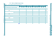
CMOS Mode timing output: pins D9 to D0 and DAV
t
PD
propagation
delay
DATA 13.6 14.9 16.4 11.9 12.9 14.4 8.0 10.8 12.4 8.2 9.7 11.3 ns
DAV -4.2--3.6--3.3--3.4-ns
t
su
set-up time - 12.5 - - 9.8 - - 6.8 - - 5.6 - ns
t
h
hold time -3.4--3.3--3.1--2.8-ns
t
r
rise time DATA
[2]
0.39 - 2.4 0.39 - 2.4 0.39 - 2.4 0.39 - 2.4 ns
DAV 0.26 - 2.4 0.26 - 2.4 0.26 - 2.4 0.26 - 2.4 ns
t
f
fall time DATA
[2]
0.19 - 2.4 0.19 - 2.4 0.19 - 2.4 0.19 - 2.4 ns