
Datasheet

ADC1015S_SER All information provided in this document is subject to legal disclaimers. © NXP B.V. 2010. All rights reserved.
Product data sheet Rev. 2 — 20 December 2010 16 of 42
NXP Semiconductors
ADC1015S series
Single 10-bit ADC; input buffer; CMOS or LVDS DDR digital outputs
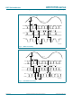
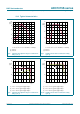
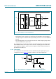
10.4 Typical characteristics
T=25C; V
DD
=3V; f
i
= 170 MHz; f
s
= 125 Msps
(1) DCS on
(2) DCS off
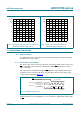
T=25C; V
DD
=3V; f
i
= 170 MHz; f
s
= 125 Msps
(1) DCS on
(2) DCS off
Fig 7. Spurious-free dynamic range as a function of
duty cycle ()
Fig 8. Signal-to-noise ratio as a function of duty
cycle ()
δ (%)
10 907030 50
001aam616
40
60
20
80
100
SFDR
(dBc)
0
(1)
(2)
δ (%)
10 907030 50
001aam615
40
20
60
80
SNR
(dBFS)
0
(1)
(2)
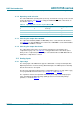
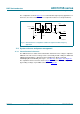
(1) T
amb
= 40 C, typical supply voltages
(2) T
amb
=+25C, typical supply voltages
(3) T
amb
=+90C, typical supply voltages
(1) T
amb
= 40 C, typical supply voltages
(2) T
amb
=+25C, typical supply voltages
(3) T
amb
=+90C, typical supply voltages
Fig 9. Spurious-free dynamic range as a function of
duty cycle ()
Fig 10. Signal-to-noise ratio as a function of duty
cycle ()
δ (%)
10 907030 50
001aam617
84
88
92
SFDR
(dBc)
80
(1)
(2)
(3)
δ (%)
10 907030 50
001aam618
40
60
80
SNR
(dBFS)
20
(1)
(2)
(3)