
Datasheet

ADC1015S_SER All information provided in this document is subject to legal disclaimers. © NXP B.V. 2010. All rights reserved.
Product data sheet Rev. 2 — 20 December 2010 19 of 42
NXP Semiconductors
ADC1015S series
Single 10-bit ADC; input buffer; CMOS or LVDS DDR digital outputs
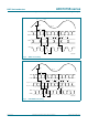
The integrated input buffer offers the following advantages:
• The kickback effect is avoided - the charge injection and glitches generated by the
S/H input stage are isolated from the input circuitry. So there’s no need for additional
filtering.
• The input capacitance is very low and constant over a wide frequency range, which
makes the ADC1015S easy to drive.
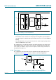
The sample phase occurs when the internal clock (derived from the clock signal on pin
CLKP/CLKM) is HIGH. The voltage is then held on the sampling capacitors. When the
clock signal goes LOW, the stage enters the hold phase and the voltage information is
transmitted to the ADC core.
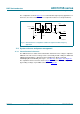
11.2.2 Transformer
The configuration of the transformer circuit is determined by the input frequency. The
configuration shown in Figure 15
would be suitable for a baseband application.
Fig 14. Input sampling circuit and input buffer
005aaa107
INP
package ESD parasitics
switch
R
on
= 15 Ω
4 pF
4 pF
sampling
capacitor
sampling
capacitor
switch
R
on
= 15 Ω
INM
8
7
internal
clock
internal
clock
INPUT
BUFFER
Fig 15. Single transformer configuration suitable for baseband applications
005aaa108
100 nF
100 nF
100 nF
100 nF
INP
INM
VCM
Analog
input
ADT1-1WT
100 nF
100 nF
50 Ω