
Datasheet


xxxxxxxxxxxxxxxxxxxxx xxxxxxxxxxxxxxxxxxxxxxxxxx xxxxxxx x x x xxxxxxxxxxxxxxxxxxxxxxxxxxxxxx xxxxxxxxxxxxxxxxxxx xx xx xxxxx
xxxxxxxxxxxxxxxxxxxxxxxxxxx xxxxxxxxxxxxxxxxxxx xxxxxx xxxxxxxxxxxxxxxxxxxxxxxxxxxxxxxxxxx xxxxxxxxxxxx x x
xxxxxxxxxxxxxxxxxxxxx xxxxxxxxxxxxxxxxxxxxxxxxxxxxxx xxxxx xxxxxxxxxxxxxxxxxxxxxxxxxxxxxxxxxxxxxxxxxxxxxxxxxx xxxxxxxx
xxxxxxxxxxxxxxxxxxxxxxxxx xxxxxxxxxxxxxxxxxxxx xxx
ADC1015S_SER All information provided in this document is subject to legal disclaimers. © NXP B.V. 2010. All rights reserved.
Product data sheet Rev. 2 — 20 December 2010 31 of 42
NXP Semiconductors
ADC1015S series
Single 10-bit ADC; input buffer; CMOS or LVDS DDR digital outputs
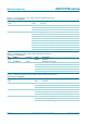
11.6.3 Register allocation map
Table 18. Register allocation map
Addr
Hex
Register name R/W Bit definition Default
Bit 7 Bit 6 Bit 5 Bit 4 Bit 3 Bit 2 Bit 1 Bit 0 Bin
0005 Reset and
operating mode
R/W SW_RST RESERVED[2:0] - - OP_MODE[1:0] 0000
0000
0006 Clock R/W - - - SE_SEL DIFF_SE - CLKDIV DCS_EN 0000
0001
0008 Internal reference R/W - - - - INTREF_EN INTREF[2:0] 0000
0000
0010 Input buffer R/W - - - - - - IB_IBIAS[1:0] - 0000
0011
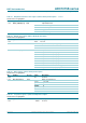
0011 Output data
standard.
R/W - - - LVDS_
CMOS
OUTBUF OUTBUS_SWAP DATA_FORMAT[1:0] 0000
0000
0012 Output clock R/W - - - - DAVINV DAVPHASE[2:0] 0000
1110
0013 Offset R/W - - DIG_OFFSET[5:0] 0000
0000
0014 Test pattern 1 R/W - - - - - TESTPAT_SEL[2:0] 0000
0000
0015 Test pattern 2 R/W TESTPAT_USER[9:2] 0000
0000
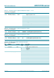
0016 Test pattern 3 R/W TESTPAT_
USER[1:0]
- - - - - - 0000
0000
0017 Fast OTR R/W - - - - FASTOTR FASTOTR_DET[2:0] 0000
0000
0020 CMOS output R/W - - - - DAV_DRV[1:0] DATA_DRV[1:0] 0000
1110
0021 LVDS DDR O/P 1 R/W - - DAVI_
x2_EN
DAVI[1:0] DATAI_x2_EN DATAI[1:0] 0000
0000
0022 LVDS DDR O/P 2 R/W - - - - BIT_BYTE_WISE LVDS_INT_TER[2:0] 0000
0000