
Datasheet


ADC1015S_SER All information provided in this document is subject to legal disclaimers. © NXP B.V. 2010. All rights reserved.
Product data sheet Rev. 2 — 20 December 2010 32 of 42
NXP Semiconductors
ADC1015S series
Single 10-bit ADC; input buffer; CMOS or LVDS DDR digital outputs
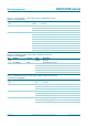
Table 19. Reset and operating mode control register (address 0005h) bit description
Default values are highlighted.
Bit Symbol Access Value Description
7 SW_RST R/W reset digital section
0no reset
1 performs a reset on SPI registers
6 to 4 RESERVED[2:0] 000 reserved
3 to 2 - 00 not used
1 to 0 OP_MODE[1:0] R/W operating mode
00 normal (Power-up)
01 Power-down
10 Sleep
11 normal (Power-up)
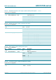
Table 20. Clock control register (address 0006h) bit description
Default values are highlighted.
Bit Symbol Access Value Description
7 to 5 - 000 not used
4 SE_SEL R/W single-ended clock input pin select
0CLKM
1CLKP
3 DIFF_SE R/W differential/single ended clock input select
0 fully differential
1 single-ended
2 - 0 not used
1 CLKDIV R/W clock input divide by 2
0disabled
1 enabled
0 DCS_EN R/W duty cycle stabilizer
0 disabled
1 enabled