
Datasheet

ADC1015S_SER All information provided in this document is subject to legal disclaimers. © NXP B.V. 2010. All rights reserved.
Product data sheet Rev. 2 — 20 December 2010 4 of 42
NXP Semiconductors
ADC1015S series
Single 10-bit ADC; input buffer; CMOS or LVDS DDR digital outputs
6. Pinning information
6.1 Pinning
6.2 Pin description
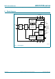
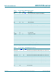
Fig 2. Pin configuration with CMOS digital outputs
selected
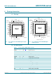
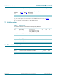
Fig 3. Pin configuration with LVDS/DDR digital
outputs selected
ADC1015S
HVQFN40
D5
D4
D3
D2
D1
D0
n.c.
n.c.
n.c.
n.c.
VDDA3V
INP
INM
AGND
VDDA5V
VCM
AGND
REFT
REFB
VDDA3V
CLKP
CLKM
DEC
PWD
D9
D8
D7
D6
VREF
SENSE
SDIO/ODS
SCLK/DFS
OTR
OGND
VDDO
n.c.
DAV
10 21
9 22
8 23
7 24
6 25
5 26
4 27
3 28
2 29
1 30
11
12
13
14
15
16
17
18
19
20
40
39
38
37
36
35
34
33
32
31
AGND
terminal 1
index area
Transparent top view
005aaa144
OE
CS
ADC1015S
HVQFN40
D4_D5_M
D4_D5_P
D2_D3_M
D2_D3_P
D0_D1_M
D0_D1_P
n.c.
n.c.
n.c.
n.c.
VDDA3V
INP
INM
AGND
VDDA5V
VCM
AGND
REFT
REFB
VDDA3V
CLKP
CLKM
DEC
PWD
D8_D9_M
D8_D9_P
D6_D7_M
D6_D7_P
VREF
SENSE
SDIO/ODS
SCLK/DFS
OTR
OGND
VDDO
n.c.
DAV
10 21
9 22
8 23
7 24
6 25
5 26
4 27
3 28
2 29
1 30
11
12
13
14
15
16
17
18
19
20
40
39
38
37
36
35
34
33
32
31
AGND
terminal 1
index area
Transparent top view
005aaa145
OE
CS
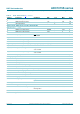
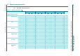
Table 2. Pin description (CMOS digital outputs)
Symbol Pin Type
[1]
Description
REFB 1 O bottom reference
REFT 2 O top reference
AGND 3 G analog ground
VCM 4 O common-mode output voltage
VDDA5V 5 P 5 V analog power supply
AGND 6 G analog ground
INM 7 I complementary analog input
INP 8 I analog input
AGND 9 G analog ground
VDDA3V 10 P 3 V analog power supply
VDDA3V 11 P 3 V analog power supply
CLKP 12 I clock input
CLKM 13 I complementary clock input
DEC 14 O regulator decoupling node
OE
15 I output enable, active LOW
PWD 16 I power down, active HIGH