
Datasheet

ADC1015S_SER All information provided in this document is subject to legal disclaimers. © NXP B.V. 2010. All rights reserved.
Product data sheet Rev. 2 — 20 December 2010 7 of 42
NXP Semiconductors
ADC1015S series
Single 10-bit ADC; input buffer; CMOS or LVDS DDR digital outputs
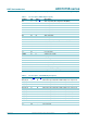
9. Static characteristics
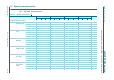
Table 6. Static characteristics
[1]
Symbol Parameter Conditions Min Typ Max Unit
Supplies
V
DDA(5V)
analog supply voltage 5 V 4.75 5.0 5.25 V
V
DDA(3V)
analog supply voltage 3 V 2.85 3.0 3.4 V
V
DDO
output supply voltage CMOS mode 1.65 1.8 3.6 V
LVDS DDR mode 2.85 3.0 3.6 V
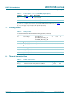
I
DDA(5V)
analog supply current 5 V f
clk
=125Msps;
f
i
=70MHz
-46-mA
I
DDA(3V)
analog supply current 3 V f
clk
=125Msps;
f
i
=70MHz
-205-mA
I
DDO
output supply current CMOS mode;
f
clk
=125Msps;
f
i
=70MHz
-10-mA
LVDS DDR mode:
f
clk
=125Msps;
f
i
=70MHz
-35-mA
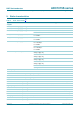
P power dissipation ADC1015S125;
analog supply only
-840-mW
ADC1015S105;
analog supply only
-770-mW
ADC1015S080;
analog supply only
-635-mW
ADC1015S065;
analog supply only
-580-mW
Power-down mode - 2 - mW
Standby mode - 40 - mW
Clock inputs: pins CLKP and CLKM
LVPECL
V
i(clk)dif
differential clock input voltage peak-to-peak - 1.6 - V
SINE wave
V
i(clk)dif
differential clock input voltage peak - 3.0 - V
LVCMOS
V
IL
LOW-level input voltage - - 0.3V
DDA(3V)
V
V
IH
HIGH-level input voltage 0.7V
DDA(3V)
--V
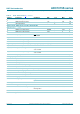
Logic inputs: pins PWD and OE
V
IL
LOW-level input voltage 0 - 0.8 V
V
IH
HIGH-level input voltage 2 - V
DDA(3V)
V
I
IL
LOW-level input current - 55 - A
I
IH
HIGH-level input current - 65 - A
Serial peripheral interface: pins CS
, SDIO/ODS, SCLK/DFS
V
IL
LOW-level input voltage 0 - 0.3V
DDA(3V)
V
V
IH
HIGH-level input voltage 0.7V
DDA(3V)
-V
DDA(3V)
V