
Datasheet

ADC1015S_SER All information provided in this document is subject to legal disclaimers. © NXP B.V. 2010. All rights reserved.
Product data sheet Rev. 2 — 20 December 2010 8 of 42
NXP Semiconductors
ADC1015S series
Single 10-bit ADC; input buffer; CMOS or LVDS DDR digital outputs
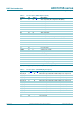
I
IL
LOW-level input current 10 - +10 A
I
IH
HIGH-level input current 50 - +50 A
C
I
input capacitance - 4 - pF
Digital outputs, CMOS mode: pins D9 to D0, OTR, DAV
Output levels, V
DDO
=3V
V
OL
LOW-level output voltage OGND - 0.2V
DDO
V
V
OH
HIGH-level output voltage 0.8V
DDO
-V
DDO
V
C
O
output capacitance high impedance;
OE
=HIGH
-3-pF
Output levels, V
DDO
=1.8V
V
OL
LOW-level output voltage OGND - 0.2V
DDO
V
V
OH
HIGH-level output voltage 0.8V
DDO
-V
DDO
V
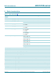
Digital outputs, LVDS mode: pins D8_D9_P to D0_D1_P, D8_D9_M to D0_D1_M, DAVP and DAVM
Output levels, V
DDO
= 3 V only, R
load
=100
V
O(offset)
output offset voltage output buffer current
set to 3.5 mA
-1.2-V
V
O(dif)
differential output voltage output buffer current
set to 3.5 mA
-350-mV
C
O
output capacitance - 3 - pF
Analog inputs: pins INP and INM
I
I
input current 5- +5A
R
I
input resistance - 550 -
C
I
input capacitance - 1.3 - pF
V
I(cm)
common-mode input voltage V
INP
=V
INM
0.9 1.5 2 V
B
i
input bandwidth - 600 - MHz
V
I(dif)
differential input voltage peak-to-peak 1 2 V
Common mode output voltage: pin VCM
V
O(cm)
common-mode output voltage - 0.5V
DDA(3V)
-V
I
O(cm)
common-mode output current - 4 - mA
I/O reference voltage: pin VREF
V
VREF
voltage on pin VREF output - 0.5 to 1 - V
input 0.5 - 1 V
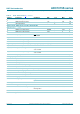
Accuracy
INL integral non-linearity 0.4 0.07 +0.4 LSB
DNL differential non-linearity guaranteed no
missing codes
0.06 0.04 +0.06 LSB
E
offset
offset error - 2- mV
E
G
gain error - 0.5 - %FS
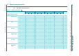
Table 6. Static characteristics
[1]
…continued
Symbol Parameter Conditions Min Typ Max Unit