
Datasheet


BF1108_BF1108R_4 © NXP B.V. 2008. All rights reserved.
Product data sheet Rev. 04 — 29 May 2008 3 of 10
NXP Semiconductors
BF1108; BF1108R
Silicon RF switches
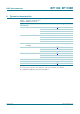
5. Limiting values
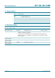
6. Thermal characteristics
[1] Soldering point of FET gate and diode anode lead.
7. Static characteristics
Table 5. Limiting values
In accordance with the Absolute Maximum Rating System (IEC 60134).
Symbol Parameter Conditions Min Max Unit
FET
V
DS
drain-source voltage - 3 V
V
SD
source-drain voltage - 3 V
V
DG
drain-gate voltage - 7 V
V
SG
source-gate voltage - 7 V
I
D
drain current - 10 mA
Diode
V
R
reverse voltage - 35 V
I
F
forward current - 100 mA
FET and diode
T
stg
storage temperature −65 +150 °C
T
j
junction temperature - 150 °C
Table 6. Thermal characteristics
Symbol Parameter Conditions Typ Unit
R
th(j-sp)
thermal resistance from junction
to solder point
[1]
250 K/W
Table 7. Static characteristics
T
j
= 25
°
C unless otherwise specified.
Symbol Parameter Conditions Min Typ Max Unit
FET
V
(BR)GSS
gate-source breakdown
voltage
V
DS
=0V; I
GS
= 0.1 mA 7 - - V
V
GS(p)
gate-source pinch-off voltage V
DS
=1V; I
D
=20µA- −3 −4V
I
DSX
drain cut-off current V
GS
= −5 V; V
DS
=2V--10µA
I
GSS
gate leakage current V
GS
= −5 V; V
DS
= 0 V - - 100 nA
R
DSon
drain-source on-state
resistance
V
GS
=0V; I
D
= 1 mA - 12 20 Ω
Diode
V
F
forward voltage I
F
= 10 mA - - 1 V
I
R
reverse current V
R
=25V --50nA
V
R
= 20 V; T
amb
=75°C--1µA