
Datasheet


BF545A_BF545B_BF545C All information provided in this document is subject to legal disclaimers. © NXP B.V. 2011. All rights reserved.
Product data sheet Rev. 4 — 15 September 2011 3 of 16
NXP Semiconductors
BF545A; BF545B; BF545C
N-channel silicon junction field-effect transistors)
5. Limiting values
[1] Device mounted on an FR4 printed-circuit board, maximum lead length 4 mm; mounting pad for the drain
lead 10 mm
2
.
6. Thermal characteristics
[1] Device mounted on an FR4 printed-circuit board, maximum lead length 4 mm; mounting pad for the drain
lead 10 mm
2
.
Table 5. Limiting values
In accordance with the Absolute Maximum Rating System (IEC 60134).
Symbol Parameter Conditions Min Max Unit
V
DS
drain-source voltage (DC) - 30 V
V
GSO
gate-source voltage open drain - 30 V
V
GDO
gate-drain voltage (DC) open source - 30 V
I
G
forward gate current (DC) - 10 mA
P
tot
total power dissipation T
amb
25 C
[1]
-250mW
T
stg
storage temperature 65 +150 C
T
j
junction temperature - 150 C
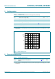
Fig 1. Power derating curve.
T
amb
(°C)
0 20015050 100
mbb688
200
100
300
400
P
tot
(mW)
0
Table 6. Thermal characteristics
Symbol Parameter Conditions Typ Unit
R
th(j-a)
thermal resistance from junction to
ambient
[1]
500 K/W