
Datasheet


BF545A_BF545B_BF545C All information provided in this document is subject to legal disclaimers. © NXP B.V. 2011. All rights reserved.
Product data sheet Rev. 4 — 15 September 2011 5 of 16
NXP Semiconductors
BF545A; BF545B; BF545C
N-channel silicon junction field-effect transistors)
8. Dynamic characteristics
Table 8. Dynamic characteristics
T
amb
= 25
C unless otherwise specified.
Symbol Parameter Conditions Min Typ Max Unit
C
iss
input capacitance V
DS
=15V; f=1MHz
V
GS
= 10 V - 1.7 - pF
V
GS
=0V - 3 - pF
C
rss
reverse transfer capacitance V
DS
=15V; f=1MHz
V
GS
= 10 V - 0.8 - pF
V
GS
= 0 V - 0.9 - pF
g
is
common source input
conductance
V
DS
=10V; I
D
=1mA
f = 100 MHz - 15 - S
f = 450 MHz - 300 - S
g
fs
common source transfer
conductance
V
DS
=10V; I
D
=1mA
f = 100 MHz - 2 - mS
f = 450 MHz - 1.8 - mS
g
rs
common source reverse
conductance
V
DS
=10V; I
D
=1mA
f = 100 MHz - 6- S
f = 450 MHz - 40 - S
g
os
common source output
conductance
V
DS
=10V; I
D
=1mA
f = 100 MHz - 30 - S
f = 450 MHz - 60 - S
V
DS
= 15 V; T
j
= 25 C. V
DS
= 15 V; V
GS
= 0 V; T
j
= 25 C.
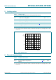
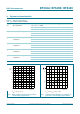
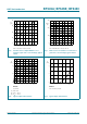
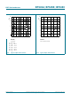
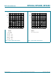
Fig 2. Drain current as a function of gate-source
cut-off voltage; typical values.
Fig 3. Forward transfer admittance as a function of
gate-source cut-off voltage; typical values.
V
GSoff
(V)
0 −8−6−2 −4
mbb467
10
20
30
I
DSS
(mA)
0
V
GSoff
(V)
0 −8−6−2 −4
mbb466
5
4.5
5.5
6
Y
fs
(mS)
4