
Datasheet


NXP Semiconductors Product specification
Dual-gate MOS-FETs BF908; BF908R
FEATURES
• High forward transfer admittance
• Short channel transistor with high forward transfer
admittance to input capacitance ratio
• Low noise gain controlled amplifier up to 1 GHz.
APPLICATIONS
• VHF and UHF applications with 12 V supply voltage,
such as television tuners and professional
communications equipment.
DESCRIPTION
Depletion type field-effect transistor in a plastic
microminiature SOT143 or SOT143R package. The
transistors are protected against excessive input voltage
surges by integrated back-to-back diodes between gates
and source.
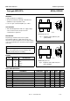
PINNING
CAUTION
The device is supplied in an antistatic package. The
gate-source input must be protected against static
discharge during transport or handling.
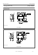
PIN SYMBOL DESCRIPTION
1 s, b source
2 d drain
3g
2
gate 2
4g
1
gate 1
Fig.1 Simplified outline (SOT143) and
symbol; BF908.
handbook, halfpage
s,b
d
g
1
g
2
43
21
Top view
BF908 marking code: %M1.
MAM039
Fig.2 Simplified outline (SOT143R) and
symbol; BF908R.
handbook, halfpage
s,b
d
g
1
g
2
MAM040
34
12
Top view
BF908R marking code: %M2.
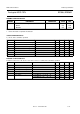
QUICK REFERENCE DATA
SYMBOL PARAMETER CONDITIONS MIN. TYP. MAX. UNIT
V
DS
drain-source voltage −−12 V
I
D
drain current −−40 mA
P
tot
total power dissipation −−200 mW
T
j
operating junction temperature −−150 °C
y
fs
forward transfer admittance 36 43 50 mS
C
ig1-s
input capacitance at gate 1 2.4 3.1 4 pF
C
rs
reverse transfer capacitance f = 1 MHz 20 30 45 pF
F noise figure f = 800 MHz − 1.5 2.5 dB
Rev. 03 - 14 November 2007
2 of 9