
Datasheet


NXP Semiconductors Product specification
Dual-gate MOS-FETs BF908; BF908R
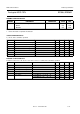
LIMITING VALUES
In accordance with the Absolute Maximum Rating System (IEC 134).
Note
1. Device mounted on a printed-circuit board.
SYMBOL PARAMETER CONDITIONS MIN. MAX. UNIT
V
DS
drain-source voltage − 12 V
I
D
drain current − 40 mA
±I
G1
gate 1 current − 10 mA
±I
G2
gate 2 current − 10 mA
P
tot
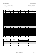
total power dissipation see Fig.3; note 1
BF908 up to T
amb
=50°C − 200 mW
BF908R up to T
amb
=40°C − 200 mW
T
stg
storage temperature −65 +150 °C
T
j
operating junction temperature − 150 °C
Fig.3 Power derating curves.
handbook, halfpage
0
50
100
150
200
250
0 50 100 150 200
BF908
BF908R
P
tot
(mW)
T
amb
( C)
o
MRC275
Rev. 03 - 14 November 2007
3 of 9