
Datasheet


BGA3018 All information provided in this document is subject to legal disclaimers. © NXP B.V. 2013. All rights reserved.
Product data sheet Rev. 3 — 26 September 2013 2 of 15
NXP Semiconductors
BGA3018
1 GHz 18 dB gain wideband amplifier MMIC
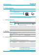
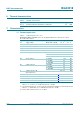
2. Pinning information
[1] This pin is DC-coupled and requires an external DC-blocking capacitor.
[2] The center metal base of the SOT89 also functions as heatsink for the power amplifier.
3. Ordering information
4. Marking
5. Limiting values
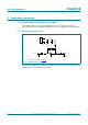
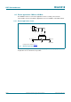
Table 2. Pinning
Pin Description Simplified outline Graphic symbol
1 RF_OUT and biasing
[1]
2GND
[2]
3RF_IN
[1]
321
sym130
2
13
Table 3. Ordering information
Type number Package
Name Description Version
BGA3018 - plastic surface-mounted package; exposed die pad
for good heat transfer; 3 leads
SOT89
OM7860 EVB 1 GHz 18 dB gain wideband amplifier application -
OM7864 EVB 5 MHz to 300 MHz 18 dB reverse amplifier application -
OM7868 EVB 40 MHz to 1006 MHz push-pull amplifier application -
OM7861 EVB BGA301x wideband variable gain amplifier application -
Table 4. Marking codes
Type number Marking code Description
BGA3018 *6Y * = W : made in China
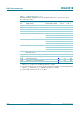
Table 5. Limiting values
In accordance with the Absolute Maximum Rating System (IEC 60134).
Symbol Parameter Conditions Min Max Unit
V
CC
supply voltage RF input AC coupled 0.6 +15 V
P
i
input power single tone - 20 dBm
T
stg
storage temperature 65 +150 C
T
j
junction temperature - 150 C
T
amb
ambient temperature 40 +85 C
V
ESD
electrostatic discharge
voltage
Human Body Model (HBM);
According JEDEC standard 22-A114E
2- kV
Charged Device Model (CDM);
According JEDEC standard 22-C101B
2- kV