
Datasheet


BGA3018 All information provided in this document is subject to legal disclaimers. © NXP B.V. 2013. All rights reserved.
Product data sheet Rev. 3 — 26 September 2013 3 of 15
NXP Semiconductors
BGA3018
1 GHz 18 dB gain wideband amplifier MMIC
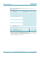
6. Thermal characteristics
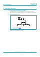
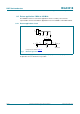
7. Characteristics
7.1 Forward application
[1] The fundamental frequencies (f
1
) and (f
2
) lay between 40 MHz and 1006 MHz. The intermodulation product
(IM3) is 2 f
2
f
1
, where f
2
=f
1
6 MHz. Input power P
i
= 20 dBm.
[2] The fundamental frequencies (f
1
) and (f
2
) lay between 40 MHz and 1006 MHz. The intermodulation product
(IM2) is f
2
f
1
, with 40 MHz < f
1
-f
2
< 1006 MHz. Input power P
i
= 20 dBm.
[3] Measured with 132 NTSC channels V
O
= 30 dBmV.
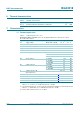
Table 6. Thermal characteristics
Symbol Parameter Conditions Typ Unit
R
th(j-sp)
thermal resistance from junction to solder point 40 K/W
Table 7. Characteristics at V
CC
= 8 V
Bandwidth 40 MHz to 1006 MHz; T
amb
= 25
C; typical values at V
CC
= 8 V; Z
S
=Z
L
=75
;
R1 = 470
; R2 = 300
.
Symbol Parameter Conditions Min Typ Max Unit
V
CC
supply voltage RF input AC coupled 7.6 8 8.4 V
I
CC(tot)
total supply current - 120 135 mA
s
21
2
insertion power gain 17 18 19 dB
SL
sl
slope straight line - 0.5 - dB
FL flatness of frequency response - 0.5 - dB
NF noise figure f = 50 MHz - 1.9 2.4 dB
f = 500 MHz - 2.1 2.6 dB
f = 1000 MHz - 2.5 3.0 dB
RL
in
input return loss f = 50 MHz - 18.5 - dB
f = 500 MHz - 20 - dB
f = 1000 MHz - 28 - dB
RL
out
output return loss f = 50 MHz - 24 - dB
f = 500 MHz - 28 - dB
f = 1000 MHz - 16 - dB
P
L(1dB)
output power at 1 dB
gain compression
23.5 25 - dBm
IP3
O
output third-order intercept point
[1]
36 40 - dBm
IP2
O
output second-order intercept point
[2]
-60-dBm
CTB composite triple beat
[3]
- 75 - dBc
CSO composite second-order distortion
[3]
- 60 - dBc