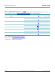
BGA7124 400 MHz to 2700 MHz 0.25 W high linearity silicon amplifier Rev. 3 — 9 September 2010 Product data sheet 1. Product profile 1.1 General description The BGA7124 MMIC is a one-stage amplifier, available in a low-cost leadless surface-mount package. It delivers 25 dBm output power at 1 dB gain compression and superior performance up to 2700 MHz.
BGA7124 NXP Semiconductors 400 MHz to 2700 MHz 0.25 W high linearity silicon amplifier 2. Pinning information 2.1 Pinning terminal 1 index area n.c. 1 VCC(RF) 2 8 ICQ_ADJ 7 RF_IN 6 SHDN 5 VCC(BIAS) BGA7124 VCC(RF) 3 n.c. 4 GND PAD 014aab046 Transparent top view Fig 1. HVSON8 package pin configuration 2.2 Pin description Table 2. Pin description Symbol Pin Description n.c.
BGA7124 NXP Semiconductors 400 MHz to 2700 MHz 0.25 W high linearity silicon amplifier 4. Functional diagram VCC SHDN 6 INPUT MATCH VCC(BIAS) ICQ_ADJ 5 8 BIAS ENABLE BANDGAP R2 V/I CONVERTER R1 RF_OUT 2, 3 VCC(RF) RF_IN 7 OUTPUT MATCH GND 014aab047 Fig 2. Functional diagram 5. Shutdown control Table 4.
BGA7124 NXP Semiconductors 400 MHz to 2700 MHz 0.25 W high linearity silicon amplifier 6. Limiting values Table 5. Limiting values In accordance with the Absolute Maximum Rating System (IEC 60134). Symbol Min Max Unit RF supply voltage [1] - 6.0 V VCC(BIAS) bias supply voltage [1] - 6.0 V ICC supply current 50 200 mA 0.
BGA7124 NXP Semiconductors 400 MHz to 2700 MHz 0.25 W high linearity silicon amplifier 7. Thermal characteristics Table 6. Symbol Rth(j-mb) [1] Thermal characteristics Parameter Conditions Typ Max Unit thermal resistance from junction to mounting base Tcase = 85 °C; VCC = 5 V; ICC = 130 mA [1] 32 - K/W defined as thermal resistance from junction to GND paddle. 8. Static characteristics Table 7. Characteristics Input and output impedances matched to 50 Ω, pin SHDN = HIGH (shutdown disabled).
BGA7124 NXP Semiconductors 400 MHz to 2700 MHz 0.25 W high linearity silicon amplifier 014aab049 170 014aab050 200 ICC (mA) ICC (mA) 170 130 140 VCC = 5 V; R1 = 0 VCC = 3.3 V; R1 = 0 110 90 80 50 1.6 2.0 2.4 2.8 3.2 3.6 50 0.9 4.0 4.4 R2 (kΩ) a. 5 V supply voltage. Fig 4. 1.4 1.9 2.4 2.9 3.4 R2 (kΩ) b. 3.3 V supply voltage Supply current as a function of the value of R2 9. Dynamic characteristics Table 8.
BGA7124 NXP Semiconductors 400 MHz to 2700 MHz 0.25 W high linearity silicon amplifier Table 8. Characteristics at VCC = 5 V …continued Input and output impedances matched to 50 Ω, pin SHDN = HIGH (shutdown disabled). Typical values at VCC = 5 V; ICC = 130 mA; Tcase = 25 °C; see Section 12 “Application information”; unless otherwise specified.
BGA7124 NXP Semiconductors 400 MHz to 2700 MHz 0.25 W high linearity silicon amplifier Table 9. Characteristics at VCC = 3.3 V Input and output impedances matched to 50 Ω, pin SHDN = HIGH (shutdown disabled). Typical values at VCC = 3.3 V; ICC = 130 mA; Tcase = 25 °C, see Section 12 “Application information”; unless otherwise specified. Symbol Parameter f frequency Gp power gain Conditions [1] f = 2445 MHz IP3O output third-order intercept point noise figure - 22.5 - dB - 13.
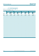
BGA7124 NXP Semiconductors 400 MHz to 2700 MHz 0.25 W high linearity silicon amplifier 9.1 Scattering parameters Table 10. Scattering parameters at 5 V, MMIC only VCC = 5 V; ICC = 130 mA; Tcase = 25 °C. f (MHz) s11 s21 s12 s22 Magnitude (ratio) Angle (degree) Magnitude (ratio) Angle (degree) Magnitude (ratio) Angle (degree) Magnitude (ratio) Angle (degree) 400 0.85 161.56 22.94 82.35 0.01 17.02 0.46 −156.50 500 0.90 159.44 11.82 82.58 0.01 27.08 0.63 176.13 600 0.90 152.
BGA7124 NXP Semiconductors 400 MHz to 2700 MHz 0.25 W high linearity silicon amplifier Table 11. Scattering parameters at 3.3 V, MMIC only VCC = 3.3 V; ICC = 130 mA; Tcase = 25 °C. f (MHz) s11 s21 s12 s22 Magnitude (ratio) Angle (degree) Magnitude (ratio) Angle (degree) Magnitude (ratio) Angle (degree) Magnitude (ratio) Angle (degree) 400 0.84 161.94 21.25 73.81 0.01 17.66 0.57 −154.41 500 0.91 159.25 11.56 79.01 0.01 28.15 0.65 178.05 600 0.90 151.98 9.67 70.71 0.
BGA7124 NXP Semiconductors 400 MHz to 2700 MHz 0.25 W high linearity silicon amplifier 12. Application information 12.1 5 V applications 12.1.1 920 MHz to 960 MHz C8 R1 J3 VCC C10 C7 C9 L2 VCC(BIAS) 50 Ω MSL1 C1 MSL2 MSL3 J1 VCC(RF) RF_IN MSL4 L1 MSL5 MSL6 MSL7 C6 50 Ω MSL8 J2 RF_OUT C2 C3 C4 BGA7124 ICQ_ADJ C5 SHDN R2 014aab051 enable See Table 14 for a list of components. PCB board specification: Rogers RO4003C; Height = 0.508 mm; εr = 3.38; Copper thickness = 35 μm.
BGA7124 NXP Semiconductors 400 MHz to 2700 MHz 0.25 W high linearity silicon amplifier 014aab054 0 014aab055 42 RLin, RLout, ISL (dB) IP3O (dBm) RLout −10 40 (1) RLin (2) (3) −20 38 ISL −30 0.92 0.93 0.94 0.95 36 0.92 0.96 0.93 0.94 0.95 0.96 f (GHz) f (GHz) Tcase = 25 °C. (1) Tcase = −40 °C. (2) Tcase = 25 °C. (3) Tcase = 85 °C. Fig 8. Input return loss, output return loss and isolation as a function of frequency Fig 9.
BGA7124 NXP Semiconductors 400 MHz to 2700 MHz 0.25 W high linearity silicon amplifier Table 14. 5 V/130 mA application list of components; 920 MHz to 960 MHz See Figure 5 and Figure 10 for component layout. Printed-Circuit Board (PCB): Rogers RO4003C stack; height = 0.508 mm; copper plating thickness = 35 μm. Component Description Value Function Remarks C1, C6 capacitor 68 pF DC blocking Murata GRM1885C1H680JA01D C2, C3 capacitor 3.
BGA7124 NXP Semiconductors 400 MHz to 2700 MHz 0.25 W high linearity silicon amplifier 12.1.2 1930 MHz to 1990 MHz VCC C6 R1 J3 C5 C7 L1 VCC(BIAS) 50 Ω MSL1 C1 MSL2 J1 VCC(RF) RF_IN MSL3 MSL4 MSL5 C4 MSL6 50 Ω J2 RF_OUT C2 C3 BGA7124 ICQ_ADJ SHDN R2 enable 014aab057 See Table 15 for a list of components. PCB board specification: Rogers RO4003C; Height = 0.508 mm; εr = 3.38; Copper thickness = 35 μm. Fig 11.
BGA7124 NXP Semiconductors 400 MHz to 2700 MHz 0.25 W high linearity silicon amplifier 014aab060 0 014aab061 40 RLin, RLout, ISL (dB) IP3O (dBm) (2) (1) −10 38 RLout (3) RLin −20 36 ISL −30 1.93 1.95 1.97 34 1.93 1.99 1.95 1.97 f (GHz) 1.99 f (GHz) Tcase = 25 °C. (1) Tcase = −40 °C. (2) Tcase = 25 °C. (3) Tcase = 85 °C. Fig 14. Input return loss, output return loss and isolation as a function of frequency Fig 15.
BGA7124 NXP Semiconductors 400 MHz to 2700 MHz 0.25 W high linearity silicon amplifier Table 15. 5 V/130 mA application list of components; 1930 MHz to 1990 MHz See Figure 11 and Figure 16 for component layout. Printed-Circuit Board (PCB): Rogers RO4003C stack; height = 0.508 mm; copper plating thickness = 35 μm. Component Description Value Function Remarks C1, C4 capacitor 15 pF DC blocking Murata GRM1885C1H150JA01D C2 capacitor 2.
BGA7124 NXP Semiconductors 400 MHz to 2700 MHz 0.25 W high linearity silicon amplifier 014aab064 30 PL(1dB) (dBm) 014aab065 20 Gp (dB) 28 18 (1) (2) 26 16 (1) (3) (2) 24 14 (3) 22 12 20 2.11 2.13 2.15 2.17 10 2.11 2.13 2.15 f (GHz) (1) Tcase = −40 °C. (1) Tcase = −40 °C. (2) Tcase = 25 °C. (2) Tcase = 25 °C. (3) Tcase = 85 °C. (3) Tcase = 85 °C. Fig 18. Output power at 1 dB gain compression as a function of frequency 014aab066 0 2.17 f (GHz) RLin, RLout, ISL (dB) Fig 19.
BGA7124 NXP Semiconductors 400 MHz to 2700 MHz 0.25 W high linearity silicon amplifier GND GND VCC enable n.c. GND J3 C7 R1 C6 J1 J2 C5 MSL4 MSL5 L1 MSL1 C1 MSL2 MSL3 C2 C4 MSL6 C3 J I HGF EDCBA 1 2 3 4 5 6 7 8 9 10 12 11 13 RF in RF out R2 014aab068 See Table 16 for a list of components. Fig 22. 5 V/130 mA application reference board; 2110 MHz to 2170 MHz Table 16. 5 V/130 mA application list of components; 2110 MHz to 2170 MHz See Figure 17 and Figure 22 for component layout.
BGA7124 NXP Semiconductors 400 MHz to 2700 MHz 0.25 W high linearity silicon amplifier Table 16. 5 V/130 mA application list of components; 2110 MHz to 2170 MHz …continued See Figure 17 and Figure 22 for component layout. Printed-Circuit Board (PCB): Rogers RO4003C stack; height = 0.508 mm; copper plating thickness = 35 μm. Component Description Value Function MSL6[1] micro stripline 1.14 mm × 0.8 mm × 10.
BGA7124 NXP Semiconductors 400 MHz to 2700 MHz 0.25 W high linearity silicon amplifier 014aab070 26 PL(1dB) (dBm) Gp (dB) (3) 24 014aab071 20 18 (2) (1) 22 16 (1) (2) 20 14 18 12 16 2.405 2.425 2.445 2.465 2.485 f (GHz) 10 2.405 (3) 2.425 (1) Tcase = −40 °C. (1) Tcase = −40 °C. (2) Tcase = 25 °C. (2) Tcase = 25 °C. (3) Tcase = 85 °C. (3) Tcase = 85 °C. Fig 24. Output power at 1 dB gain compression as a function of frequency 014aab072 0 RLin, RLout, ISL (dB) 2.445 2.465 2.
BGA7124 NXP Semiconductors 400 MHz to 2700 MHz 0.25 W high linearity silicon amplifier GND GND VCC enable n.c. GND J3 C8 R1 C7 J1 J2 C6 L1 MSL1 C1 MSL2 MSL3 C2 C3 J I HGF EDCBA MSL4 C4 C5 MSL5 1 2 3 4 5 6 7 8 9 10 12 11 13 RF in RF out R2 014aab074 See Table 17 for a list of components. Fig 28. 5 V/130 mA application reference board; 2405 MHz to 2485 MHz Table 17. 5 V/130 mA application list of components; 2405 MHz to 2485 MHz See Figure 23 and Figure 28 for component layout.
BGA7124 NXP Semiconductors 400 MHz to 2700 MHz 0.25 W high linearity silicon amplifier Table 17. 5 V/130 mA application list of components; 2405 MHz to 2485 MHz …continued See Figure 23 and Figure 28 for component layout. Printed-Circuit Board (PCB): Rogers RO4003C stack; height = 0.508 mm; copper plating thickness = 35 μm. Component Description Value Function MSL5[1] micro stripline 1.14 mm × 0.8 mm × 10.95 mm output match R1 resistor 2.
BGA7124 NXP Semiconductors 400 MHz to 2700 MHz 0.25 W high linearity silicon amplifier 014aab076 30 PL(1dB) (dBm) 014aab077 28 Gp (dB) 28 26 26 24 (1) (2) (1) (2) 24 (3) 22 (3) 22 20 20 0.92 0.93 0.94 0.95 0.96 18 0.92 0.93 0.94 0.95 f (GHz) (1) Tcase = −40 °C. (1) Tcase = −40 °C. (2) Tcase = 25 °C. (2) Tcase = 25 °C. (3) Tcase = 85 °C. (3) Tcase = 85 °C. Fig 30. Output power at 1 dB gain compression as a function of frequency 014aab078 0 RLin, RLout, ISL (dB) Fig 31.
BGA7124 NXP Semiconductors 400 MHz to 2700 MHz 0.25 W high linearity silicon amplifier GND GND VCC enable n.c. GND J3 C9 R1 C8 J1 J2 MSL2 MSL4 C7 MSL6 MSL7 L2 MSL1 C1 L1 MSL3 C2 C3 C6 C4 J I HGF EDCBA MSL8 C5 1 2 3 4 5 6 7 8 9 10 12 11 13 MSL5 RF in RF out R2 014aab080 See Table 18 for a list of components. Fig 34. 3.3 V/130 mA application reference board; 920 MHz to 960 MHz Table 18. 3.
BGA7124 NXP Semiconductors 400 MHz to 2700 MHz 0.25 W high linearity silicon amplifier Table 18. 3.3 V/130 mA application list of components; 920 MHz to 960 MHz …continued See Figure 29 and Figure 34 for component layout. Printed-Circuit Board (PCB): Rogers RO4003C stack; height = 0.508 mm; copper plating thickness = 35 μm. Component Description Value Function MSL6[1] micro stripline 1.14 mm × 0.8 mm × 2.4 mm output match MSL7[1] micro stripline 1.14 mm × 0.8 mm × 2.
BGA7124 NXP Semiconductors 400 MHz to 2700 MHz 0.25 W high linearity silicon amplifier 014aab082 26 PL(1dB) (dBm) 014aab083 20 Gp (dB) 24 18 (3) (2) 22 16 (1) (1) (2) 20 14 (3) 18 12 16 2.405 2.425 2.445 2.465 2.485 f (GHz) 10 2.405 2.425 (1) Tcase = −40 °C. (1) Tcase = −40 °C. (2) Tcase = 25 °C. (2) Tcase = 25 °C. (3) Tcase = 85 °C. (3) Tcase = 85 °C. Fig 36. Output power at 1 dB gain compression as a function of frequency 014aab084 0 RLin, RLout, ISL (dB) 2.445 2.465 2.
BGA7124 NXP Semiconductors 400 MHz to 2700 MHz 0.25 W high linearity silicon amplifier GND GND VCC enable n.c. GND J3 C8 R1 C7 J1 J2 C6 L1 MSL1 C1 MSL2 MSL3 C2 C3 J I HGF EDCBA MSL4 C4 C5 MSL5 1 2 3 4 5 6 7 8 9 10 12 11 13 RF in RF out R2 014aab086 See Table 19 for a list of components. Fig 40. 3.3 V/130 mA application reference board; 2405 MHz to 2485 MHz Table 19. 3.3 V/130 mA application list of components; 2405 MHz to 2485 MHz See Figure 35 and Figure 40 for component layout.
BGA7124 NXP Semiconductors 400 MHz to 2700 MHz 0.25 W high linearity silicon amplifier Table 19. 3.3 V/130 mA application list of components; 2405 MHz to 2485 MHz …continued See Figure 35 and Figure 40 for component layout. Printed-Circuit Board (PCB): Rogers RO4003C stack; height = 0.508 mm; copper plating thickness = 35 μm. Component Description Value MSL5[1] micro stripline 1.14 mm × 0.8 mm × 10.95 mm output match R1 resistor 2.
BGA7124 NXP Semiconductors 400 MHz to 2700 MHz 0.25 W high linearity silicon amplifier 13. Package outline HVSON8: plastic thermal enhanced very thin small outline package; no leads; 8 terminals; body 3 x 3 x 0.85 mm SOT908-1 0 1 2 mm scale X B D A E A A1 c detail X terminal 1 index area e1 terminal 1 index area e v w b 1 4 M M C C A B C y1 C y L exposed tie bar (4×) Eh exposed tie bar (4×) 8 5 Dh DIMENSIONS (mm are the original dimensions) UNIT A(1) max.
BGA7124 NXP Semiconductors 400 MHz to 2700 MHz 0.25 W high linearity silicon amplifier 14. Abbreviations Table 20.
BGA7124 NXP Semiconductors 400 MHz to 2700 MHz 0.25 W high linearity silicon amplifier 16. Legal information 16.1 Data sheet status Document status[1][2] Product status[3] Definition Objective [short] data sheet Development This document contains data from the objective specification for product development. Preliminary [short] data sheet Qualification This document contains data from the preliminary specification.
BGA7124 NXP Semiconductors 400 MHz to 2700 MHz 0.25 W high linearity silicon amplifier Non-automotive qualified products — Unless this data sheet expressly states that this specific NXP Semiconductors product is automotive qualified, the product is not suitable for automotive use. It is neither qualified nor tested in accordance with automotive testing or application requirements.
BGA7124 NXP Semiconductors 400 MHz to 2700 MHz 0.25 W high linearity silicon amplifier 18. Contents 1 1.1 1.2 1.3 1.4 2 2.1 2.2 3 4 5 6 7 8 8.1 9 9.1 10 11 12 12.1 12.1.1 12.1.2 12.1.3 12.1.4 12.2 12.2.1 12.2.2 12.3 13 14 15 16 16.1 16.2 16.3 16.4 17 18 Product profile . . . . . . . . . . . . . . . . . . . . . . . . . . 1 General description . . . . . . . . . . . . . . . . . . . . . 1 Features and benefits . . . . . . . . . . . . . . . . . . . . 1 Applications . . . . . . . . . . . . . . . . . . . . . .