
Datasheet


BGA7124 All information provided in this document is subject to legal disclaimers. © NXP B.V. 2010. All rights reserved.
Product data sheet Rev. 3 — 9 September 2010 2 of 33
NXP Semiconductors
BGA7124
400 MHz to 2700 MHz 0.25 W high linearity silicon amplifier
2. Pinning information
2.1 Pinning
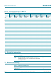
2.2 Pin description
[1] This pin is DC-coupled and requires an external DC-blocking capacitor.
[2] RF decoupled.
[3] The center metal base of the SOT908-1 also functions as heatsink for the power amplifier.
3. Ordering information
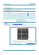
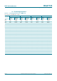
Fig 1. HVSON8 package pin configuration
014aab046
V
CC(BIAS)
SHDNV
CC(RF)
RF_INV
CC(RF)
ICQ_ADJ
GND PAD
n.c.
Transparent top view
54
63
72
81
terminal 1
index area
BGA7124
n.c.
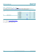
Table 2. Pin description
Symbol Pin Description
n.c. 1, 4 not connected
V
CC(RF)
2, 3 RF output for the power amplifier and DC supply input for the
RF transistor collector
[1]
V
CC(BIAS)
5 bias supply voltage
[2]
SHDN 6 shutdown control function enabled/disabled
RF_IN 7 RF input for the power amplifier
[1]
ICQ_ADJ 8 quiescent collector current adjustment controlled by an external resistor
GND GND pad RF and DC ground
[3]
Table 3. Ordering information
Type number Package
Name Description Version
BGA7124 HVSON8 plastic thermal enhanced very thin small outline
package; no leads; 8 terminals; body 3 × 3 × 0.85 mm
SOT908-1