
Datasheet


BGA7124 All information provided in this document is subject to legal disclaimers. © NXP B.V. 2010. All rights reserved.
Product data sheet Rev. 3 — 9 September 2010 3 of 33
NXP Semiconductors
BGA7124
400 MHz to 2700 MHz 0.25 W high linearity silicon amplifier
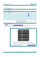
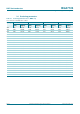
4. Functional diagram
5. Shutdown control
Fig 2. Functional diagram
BANDGAP
OUTPUT MATCH
INPUT MATCH
BIAS
ENABLE
V/I
CONVERTER
RF_OUT
GND
R1
R2
RF_IN
SHDN
V
CC
ICQ_ADJ
6
7
58
2, 3
014aab047
V
CC(BIAS)
V
CC(RF)
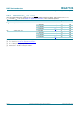
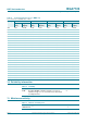
Table 4. Shutdown control settings
Mode Mode description Function description Pin
SHDN
V
ctrl(sd)
(V) I
ctrl(sd)
(μA)
Min Max Min Max
Idle medium power MMIC fully off;
minimal supply current
shutdown control enabled 0 0 0.7 - 2
TX medium power MMIC transmit mode shutdown control disabled 1 2.5 V
CC(BIAS)
-9