
Datasheet


BGA7124 All information provided in this document is subject to legal disclaimers. © NXP B.V. 2010. All rights reserved.
Product data sheet Rev. 3 — 9 September 2010 4 of 33
NXP Semiconductors
BGA7124
400 MHz to 2700 MHz 0.25 W high linearity silicon amplifier
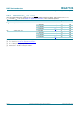
6. Limiting values
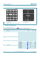
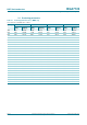
[1] See Figure 3 for safe operating area.
[2] The supply current is adjustable; see Section 8.1 “
Supply current adjustment”.
[3] If V
ctrl(sd)
exceeds V
CC(BIAS)
, the internal ESD circuit can be damaged. To prevent this, it is recommended that the I
ctrl(sd)
is limited to
20 mA. If the SHDN function is not used, the SHDN pin should be connected to the V
CC(BIAS)
pin.
Table 5. Limiting values
In accordance with the Absolute Maximum Rating System (IEC 60134).
Symbol Parameter Conditions Min Max Unit
V
CC(RF)
RF supply voltage
[1]
-6.0 V
V
CC(BIAS)
bias supply voltage
[1]
-6.0 V
I
CC
supply current
[1][2]
50 200 mA
V
ctrl(sd)
shutdown control voltage
[3]
0.0 V
CC(BIAS)
V
P
i(RF)
RF input power - 20 dBm
T
case
case temperature −40 +85 °C
T
j
junction temperature - 150 °C
V
ESD
electrostatic discharge voltage Human Body Model (HBM);
According JEDEC standard 22-A114E
- 2000 V
Charged Device Model (CDM);
According JEDEC standard 22-C101B
- 500 V
Exceeding the safe operating area limits may cause serious damage to the product.
The impact on I
CC
due to the spread of the external ICQ resistor (R2) should be taken into account.
The product-spread on I
CC
should be taken into account (see Section 8 “Static characteristics”).
Fig 3. BGA7124 DC safe operating area
V
CC(RF)
(V)
276453
014aab048
150
100
200
250
I
CC
(mA)
50