
Datasheet


BGA7124 All information provided in this document is subject to legal disclaimers. © NXP B.V. 2010. All rights reserved.
Product data sheet Rev. 3 — 9 September 2010 8 of 33
NXP Semiconductors
BGA7124
400 MHz to 2700 MHz 0.25 W high linearity silicon amplifier
[1] Operation outside this range is possible but not guaranteed.
[2] I
CC
= 160 mA; see Section 12 “Application information”.
[3] P
L
= 11 dBm per tone; spacing = 1 MHz.
[4] Defined at P
i
= −40 dBm; small signal conditions.
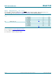
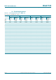
Table 9. Characteristics at V
CC
= 3.3 V
Input and output impedances matched to 50
Ω
, pin SHDN = HIGH (shutdown disabled). Typical values at V
CC
=3.3V;
I
CC
= 130 mA; T
case
=25
°
C, see Section 12 “Application information”; unless otherwise specified.
Symbol Parameter Conditions Min Typ Max Unit
f frequency
[1]
400 - 2700 MHz
G
p
power gain for small signals
f = 940 MHz - 22.5 - dB
f = 2445 MHz
[2]
-13.8- dB
P
L(1dB)
output power at 1 dB gain compression f = 940 MHz - 23.5 - dBm
f = 2445 MHz
[2]
-22.0- dBm
IP3
O
output third-order intercept point f = 940 MHz
[3]
-36.4- dBm
f = 2445 MHz
[2][3]
-35.2- dBm
NF noise figure f = 940 MHz
[4]
-5.5- dB
f = 2445 MHz
[2][4]
-5.5- dB
RL
in
input return loss f = 940 MHz - −15 - dB
f = 2445 MHz
[2]
- −10 - dB
RL
out
output return loss f = 940 MHz - −9- dB
f = 2445 MHz
[2]
- −25 - dB