56F807 Data Sheet Preliminary Technical Data 56F800 16-bit Digital Signal Controllers DSP56F807 Rev. 16 09/2007 freescale.
Document Revision History Version History Rev. 16 Description of Change Added revision history. Added this text to footnote 2 in Table 3-8: “However, the high pulse width does not have to be any particular percent of the low pulse width.
56F807 General Description • Up to 40 MIPS at 80MHz core frequency • Two 6 channel PWM Modules • DSP and MCU functionality in a unified, C-efficient architecture • Four 4 channel, 12-bit ADCs • Two Quadrature Decoders • Hardware DO and REP loops • CAN 2.
Part 1 Overview 1.1 56F807 Features 1.1.1 • • • • • • • • • • • • • • 1.1.
6F807 Description • • • • • • • • • • • 1.1.4 • • • • Two dedicated General Purpose Quad Timers totaling six pins: Timer C with two pins and Timer D with four pins CAN 2.
A total of 2K words of Boot Flash is incorporated for easy customer-inclusion of field-programmable software routines that can be used to program the main Program and Data Flash memory areas. Both Program and Data Flash memories can be independently bulk erased or erased in page sizes of 256 words. The Boot Flash memory can also be either bulk or page erased. A key application-specific feature of the 56F807 is the inclusion of two Pulse Width Modulator (PWM) modules.
Product Documentation 1.4 Product Documentation The four documents listed in Table 1-1 are required for a complete description and proper design with the 56F807. Documentation is available from local Freescale distributors, Freescale Semiconductor sales offices, Freescale Literature Distribution Centers, or online at http://www.freescale.com.
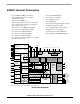
Part 2 Signal/Connection Descriptions 2.1 Introduction The input and output signals of the 56F807 are organized into functional groups, as shown in Table 2-1 and as illustrated in Figure 2-1. In Table 2-2 through Table 2-19, each table row describes the signal or signals present on a pin.
Introduction Power Port Ground Port Power Port Ground Port VDD 8 VSS 10* VDDA 3 VSSA 3 Other Supply Ports VCAPC PLL and Clock EXTAL VPP XTAL CLKO A0-A5 External Address Bus or GPIO External Data Bus A6-7 (GPIOE2-E3) A8-15 (GPIOA0-A7) D0–D15 PS DS External Bus Control RD WR PHASEA0 (TA0) Quadrature Decoder or Quad Timer A Quadrature Decoder1 or Quad Timer B PHASEB0 (TA1) 2 GPIOB0–7 6 GPIOD0–5 6 PWMA0-5 3 ISA0-2 4 FAULTA0-3 6 PWMB0-5 3 ISB0-2 4 FAULTB0-3 1 SCLK (GPIO
2.2 Power and Ground Signals Table 2-2 Power Inputs No. of Pins Signal Name Signal Description 8 VDD Power—These pins provide power to the internal structures of the chip, and should all be attached to VDD. 3 VDDA Analog Power—These pins is a dedicated power pin for the analog portion of the chip and should be connected to a low noise 3.3V supply. Table 2-3 Grounds No.
Clock and Phase Locked Loop Signals 2.3 Clock and Phase Locked Loop Signals Table 2-5 PLL and Clock No. of Pins Signal Name Signal Type State During Reset 1 EXTAL Input Input 1 XTAL Input/ Output Chip-driven Signal Description External Crystal Oscillator Input—This input should be connected to an 8MHz external crystal or ceramic resonator. For more information, please refer to Section 3.4.
Table 2-7 Data Bus Signals No. of Pins Signal Name Signal Type State During Reset 16 D0–D15 Input/O utput Tri-stated Signal Description Data Bus— D0–D15 specify the data for external program or data memory accesses. D0–D15 are tri-stated when the external bus is inactive. Internal pullups may be active. Table 2-8 Bus Control Signals No. of Pins Signal Name Signal Type State During Reset 1 PS Output Tri-stated Program Memory Select—PS is asserted low for external program memory access.
GPIO Signals Table 2-9 Interrupt and Program Control Signals (Continued) No. of Pins Signal Name Signal Type State During Reset 1 RSTO Output Output 1 RESET Input (Schmitt) Input Signal Description Reset Output—This output reflects the internal reset state of the chip. Reset—This input is a direct hardware reset on the processor. When RESET is asserted low, the device is initialized and placed in the Reset state. A Schmitt trigger input is used for noise immunity.
2.7 Pulse Width Modulator (PWM) Signals Table 2-11 Pulse Width Modulator (PWMA and PWMB) Signals No. of Pins Signal Name Signal Type State During Reset 6 PWMA0-5 Output Tri- stated 3 ISA0-2 Input (Schmitt) Input ISA0-2— These three input current status pins are used for top/bottom pulse width correction in complementary channel operation for PWMA.
Serial Peripheral Interface (SPI) Signals 2.8 Serial Peripheral Interface (SPI) Signals Table 2-12 Serial Peripheral Interface (SPI) Signals No. of Pins Signal Name Signal Type State During Reset 1 MISO Input/ Output Input SPI Master In/Slave Out (MISO)—This serial data pin is an input to a master device and an output from a slave device. The MISO line of a slave device is placed in the high-impedance state if the slave device is not selected.
2.9 Quadrature Decoder Signals Table 2-13 Quadrature Decoder (Quad Dec0 and Quad Dec1) Signals No.
Serial Communications Interface (SCI) Signals 2.10 Serial Communications Interface (SCI) Signals Table 2-14 Serial Peripheral Interface (SPI) Signals No. of Pins Signal Name Signal Type State During Reset 1 MISO Input/ Output Input SPI Master In/Slave Out (MISO)—This serial data pin is an input to a master device and an output from a slave device. The MISO line of a slave device is placed in the high-impedance state if the slave device is not selected.
Table 2-15 Serial Communications Interface (SCI0 and SCI1) Signals No. of Pins Signal Name Signal Type State During Reset 1 TXD0 Output Input Transmit Data (TXD0)—transmit data output GPIOE0 Input/Outp ut Input Port E GPIO—This pin is a General Purpose I/O (GPIO) pin that can individually be programmed as input or output pin. Signal Description After reset, the default state is SCI output.
Analog-to-Digital Converter (ADC) Signals 2.12 Analog-to-Digital Converter (ADC) Signals Table 2-17 Analog to Digital Converter Signals No. of Pins Signal Name Signal Type State During Reset 4 ANA0-3 Input Input ANA0-3—Analog inputs to ADCA channel 1 4 ANA4-7 Input Input ANA4-7—Analog inputs to ADCA channel 2 2 VREF Input Input VREF—Analog reference voltage for ADC. Must be set to VDDA-0.3V for optimal performance.
2.14 JTAG/OnCE Table 2-19 JTAG/On-Chip Emulation (OnCE) Signals No. of Pins Signal Name Signal Type State During Reset 1 TCK Input (Schmitt) Input, pulled low internally 1 TMS Input (Schmitt) Input, pulled Test Mode Select Input—This input pin is used to sequence the JTAG high internally TAP controller’s state machine. It is sampled on the rising edge of TCK and has an on-chip pull-up resistor.
General Characteristics damage to the device. The 56F807 DC/AC electrical specifications are preliminary and are from design simulations. These specifications may not be fully tested or guaranteed at this early stage of the product life cycle. Finalized specifications will be published after complete characterization and device qualifications have been completed. CAUTION This device contains protective circuitry to guard against damage due to high static voltage or electrical fields.
Table 3-2 Recommended Operating Conditions Characteristic Symbol Min Typ Max Unit Voltage difference VSS to VSSA ΔVSS -0.1 - 0.1 V ADC reference voltage VREF 2.7 – VDDA V TA –40 – 85 °C Ambient operating temperature Table 3-3 Thermal Characteristics6 Value Characteristic Comments Junction to ambient Natural convection Junction to ambient (@1m/sec) Symbol Unit Notes 63.4 °C/W 2 35.4 60.3 °C/W 2 160-pin LQFP 160 MBGA RθJA 38.
DC Electrical Characteristics 4. Thermal Characterization Parameter, Psi-JT (ΨJT ), is the “resistance” from junction to reference point thermocouple on top center of case as defined in JESD51-2. ΨJT is a useful value to use to estimate junction temperature in steady state customer environments. 5.
Table 3-4 DC Electrical Characteristics (Continued) Operating Conditions: VSS = VSSA = 0 V, VDD = VDDA = 3.0–3.6 V, TA = –40° to +85°C, CL ≤ 50pF, fop = 80MHz Characteristic Symbol Min Typ Max Unit Output Low Voltage (at IOL) VOL — — 0.
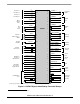
AC Electrical Characteristics 250 IDD Analog IDD Digital IDD Total 200 IDD (mA) 150 100 50 0 10 20 30 40 60 50 70 80 Freq. (MHz) Figure 3-1 Maximum Run IDD vs. Frequency (see Note 6. in Table 3-14) 3.3 AC Electrical Characteristics Timing waveforms in Section 3.3 are tested using the VIL and VIH levels specified in the DC Characteristics table. In Figure 3-2 the levels of VIH and VIL for an input signal are shown.
Data2 Valid Data1 Valid Data1 Data3 Valid Data2 Data3 Data Tri-stated Data Invalid State Data Active Data Active Figure 3-3 Signal States Table 3-5 Flash Memory Truth Table Mode XE1 YE2 SE3 OE4 PROG5 ERASE6 MAS17 NVSTR8 Standby L L L L L L L L Read H H H H L L L L Word Program H H L L H L L H Page Erase H L L L L H L H Mass Erase H L L L L H H H 1. X address enable, all rows are disabled when XE=0 2.
AC Electrical Characteristics Table 3-7 Flash Timing Parameters Operating Conditions: VSS = VSSA = 0 V, VDD = VDDA = 3.0–3.
IFREN XADR XE Tadh YADR YE DIN Tads PROG Tnvs Tprog Tpgh NVSTR Tpgs Tnvh Trcv Thv Figure 3-4 Flash Program Cycle IFREN XADR XE YE=SE=OE=MAS1=0 ERASE Tnvs NVSTR Tnvh Terase Trcv Figure 3-5 Flash Erase Cycle 56F807 Technical Data Technical Data, Rev.
External Clock Operation IFREN XADR XE MAS1 YE=SE=OE=0 ERASE Tnvs NVSTR Tnvh1 Tme Trcv Figure 3-6 Flash Mass Erase Cycle 3.4 External Clock Operation The 56F807 system clock can be derived from an external crystal or an external system clock signal. To generate a reference frequency using the internal oscillator, a reference crystal must be connected between the EXTAL and XTAL pins. 3.4.
as a typical circuit board trace capacitance the parallel load capacitance presented to the crystal is 9pF as determined by the following equation: CL1 * CL2 CL = CL1 + CL2 12 * 12 + Cs = + 3 = 6 + 3 = 9pF 12 + 12 This is the value load capacitance that should be used when selecting a crystal and determining the actual frequency of operation of the crystal oscillator circuit.
External Clock Operation 3.4.3 External Clock Source The recommended method of connecting an external clock is given in Figure 3-9. The external clock source is connected to XTAL and the EXTAL pin is grounded. 56F807 XTAL EXTAL External Clock VSS Figure 3-9 Connecting an External Clock Signal Table 3-8 External Clock Operation Timing Requirements5 Operating Conditions: VSS = VSSA = 0 V, VDD = VDDA = 3.0–3.
3.4.4 Phase Locked Loop Timing Table 3-9 PLL Timing Operating Conditions: VSS = VSSA = 0 V, VDD = VDDA = 3.0–3.6 V, TA = –40° to +85°C Characteristic Symbol Min Typ Max Unit fosc 4 8 10 MHz fout/2 40 — 110 MHz PLL stabilization time3 0o to +85oC tplls — 1 10 ms PLL stabilization time3 -40o to 0oC tplls — 100 200 ms External reference crystal frequency for the PLL1 PLL output frequency2 1.
External Bus Asynchronous Timing 3.5 External Bus Asynchronous Timing Table 3-10 External Bus Asynchronous Timing1,2 Operating Conditions: VSS = VSSA = 0 V, VDD = VDDA = 3.0–3.6 V, TA = –40° to +85°C, CL ≤ 50pF, fop = 80MHz Symbol Min Max Unit Address Valid to WR Asserted tAWR 6.5 — ns WR Width Asserted Wait states = 0 Wait states > 0 tWR 7.5 (T*WS)+7.5 — — ns ns WR Asserted to D0–D15 Out Valid tWRD — T + 4.2 ns Data Out Hold Time from WR Deasserted tDOH 4.
1. Timing is both wait state and frequency dependent. In the formulas listed, WS = the number of wait states and T = Clock Period. For 80MHz operation, T = 12.5ns. 2. Parameters listed are guaranteed by design. To calculate the required access time for an external memory for any frequency < 80MHz, use this formula: Top = Clock period @ desired operating frequency WS = Number of wait states Memory Access Time = (Top*WS) + (Top- 11.
Reset, Stop, Wait, Mode Select, and Interrupt Timing 3.6 Reset, Stop, Wait, Mode Select, and Interrupt Timing Table 3-11 Reset, Stop, Wait, Mode Select, and Interrupt Timing1,5 Operating Conditions: VSS = VSSA = 0 V, VDD = VDDA = 3.0–3.
RESET tRA tRAZ tRDA A0–A15, D0–D15 First Fetch PS, DS, RD, WR First Fetch Figure 3-12 Asynchronous Reset Timing IRQA, IRQB tIRW Figure 3-13 External Interrupt Timing (Negative-Edge-Sensitive) A0–A15, PS, DS, RD, WR First Interrupt Instruction Execution tIDM IRQA, IRQB a) First Interrupt Instruction Execution General Purpose I/O Pin tIG IRQA, IRQB b) General Purpose I/O Figure 3-14 External Level-Sensitive Interrupt Timing 56F807 Technical Data Technical Data, Rev.
Reset, Stop, Wait, Mode Select, and Interrupt Timing IRQA, IRQB tIRI A0–A15, PS, DS, RD, WR First Interrupt Vector Instruction Fetch Figure 3-15 Interrupt from Wait State Timing tIW IRQA tIF A0–A15, PS, DS, RD, WR First Instruction Fetch Not IRQA Interrupt Vector Figure 3-16 Recovery from Stop State Using Asynchronous Interrupt Timing tIRQ IRQA tII A0–A15 PS, DS, RD, WR First IRQA Interrupt Instruction Fetch Figure 3-17 Recovery from Stop State Using IRQA Interrupt Service RSTO tRSTO Figure
3.7 Serial Peripheral Interface (SPI) Timing Table 3-12 SPI Timing1 Operating Conditions: VSS = VSSA = 0 V, VDD = VDDA = 3.0–3.6 V, TA = –40° to +85°C, CL ≤ 50pF, fOP = 80MHz Characteristic Symbol Cycle time Master Slave Min Max Unit 50 25 — — ns ns — 25 — — ns ns — 100 — — ns ns 17.6 12.5 — — ns ns 24.
Serial Peripheral Interface (SPI) Timing SS SS is held High on master (Input) tC tR tF tCL SCLK (CPOL = 0) (Output) tCH tF tR tCL SCLK (CPOL = 1) (Output) tDH tCH tDS MISO (Input) MSB in Bits 14–1 tDI MOSI (Output) LSB in tDV Master MSB out Bits 14–1 tDI(ref) Master LSB out tR tF Figure 3-19 SPI Master Timing (CPHA = 0) SS SS is held High on master (Input) tC tF tR tCL SCLK (CPOL = 0) (Output) tCH tF tCL SCLK (CPOL = 1) (Output) tCH tDS tR MISO (Input) MSB in tDV(ref)
SS (Input) tC tF tCL SCLK (CPOL = 0) (Input) tELG tR tCH tELD tCL SCLK (CPOL = 1) (Input) tCH tA MISO (Output) Slave MSB out tDS tF tR tD Bits 14–1 Slave LSB out tDV tDI tDI tDH MOSI (Input) MSB in Bits 14–1 LSB in Figure 3-21 SPI Slave Timing (CPHA = 0) SS (Input) tF tC tR tCL SCLK (CPOL = 0) (Input) tCH tELG tELD tCL SCLK (CPOL = 1) (Input) tDV tCH tR tA MISO (Output) Slave MSB out Bits 14–1 tDV tDS MOSI (Input) tD tF tDH MSB in Bits 14–1 Slave LSB out tDI
Quad Timer Timing 3.8 Quad Timer Timing Table 3-13 Timer Timing1, 2 Operating Conditions: VSS = VSSA = 0 V, VDD = VDDA = 3.0–3.6 V, TA = –40° to +85°C, CL ≤ 50pF, fOP = 80MHz Characteristic Symbol Min Max Unit PIN 4T + 6 — ns Timer input high/low period PINHL 2T + 3 — ns Timer output period POUT 2T — ns POUTHL 1T — ns Timer input period Timer output high/low period 1. In the formulas listed, T = the clock cycle. For 80MHz operation, T = 12.5ns. 2.
3.9 Quadrature Decoder Timing Table 3-14 Quadrature Decoder Timing1, 2 Operating Conditions: VSS = VSSA = 0 V, VDD = VDDA = 3.0–3.6 V, TA = –40° to +85°C, CL ≤ 50pF, fOP = 80MHz Characteristic Symbol Min Max Unit Quadrature input period PIN 8T + 12 — ns Quadrature input high/low period PHL 4T + 6 — ns Quadrature phase period PPH 2T + 3 — ns 1. In the formulas listed, T = the clock cycle. For 80MHz operation, T=12.5ns. VSS = 0V, VDD = 3.0–3.6V, TA = –40° to +85°C, CL ≤ 50pF. 2.
Serial Communication Interface (SCI) Timing 3.10 Serial Communication Interface (SCI) Timing Table 3-15 SCI Timing4 Operating Conditions: VSS = VSSA = 0 V, VDD = VDDA = 3.0–3.6 V, TA = –40° to +85°C, CL ≤ 50pF, fOP = 80MHz Characteristic Symbol Min Max Unit BR — (fMAX*2.5)/(80) Mbps RXD2 Pulse Width RXDPW 0.965/BR 1.04/BR ns TXD3 Pulse Width TXDPW 0.965/BR 1.04/BR ns Baud Rate1 1. fMAX is the frequency of operation of the system clock in MHz. 2.
3.11 Analog-to-Digital Converter (ADC) Characteristics Table 3-16 ADC Characteristics Operating Conditions: VSS = VSSA = 0 V, VDD = VDDA = 3.0–3.6 V, VREF = VDD-0.3V, ADCDIV = 4, 9, or 14, (for optimal performance), ADC clock = 4MHz, 3.0–3.6 V, TA = –40° to +85°C, CL ≤ 50pF, fOP = 80MHz Characteristic Symbol Min Typ Max Unit VADCIN 01 — VREF2 V Resolution RES 12 — 12 Bits Integral Non-Linearity3 INL — +/- 2.5 +/- 4 LSB4 Differential Non-Linearity DNL — +/- 0.
Controller Area Network (CAN) Timing . ADC analog input 3 1 2 4 1. Parasitic capacitance due to package, pin to pin, and pin to package base coupling. (1.8pf) 2. Parasitic capacitance due to the chip bond pad, ESD protection devices and signal routing. (2.04pf) 3. Equivalent resistance for the ESD isolation resistor and the channel select mux. (500 ohms) 4. Sampling capacitor at the sample and hold circuit.
3.13 JTAG Timing Table 3-18 JTAG Timing1, 3 Operating Conditions: VSS = VSSA = 0 V, VDD = VDDA = 3.0–3.6 V, TA = –40° to +85°C, CL ≤ 50pF, fOP = 80MHz Characteristic Symbol Min Max Unit fOP DC 10 MHz TCK cycle time tCY 100 — ns TCK clock pulse width tPW 50 — ns TMS, TDI data set-up time tDS 0.4 — ns TMS, TDI data hold time tDH 1.2 — ns TCK low to TDO data valid tDV — 26.6 ns TCK low to TDO tri-state tTS — 23.
JTAG Timing TCK (Input) tDS TDI TMS (Input) tDH Input Data Valid tDV TDO (Output) Output Data Valid tTS TDO (Output) tDV TDO (Output) Output Data Valid Figure 3-30 Test Access Port Timing Diagram TRST (Input) tTRST Figure 3-31 TRST Timing Diagram DE tDE Figure 3-32 OnCE—Debug Event 56F807 Technical Data Technical Data, Rev.
Part 4 Packaging 4.1 Package and Pin-Out Information 56F807 DE VSS ISA2 ISA1 ISA0 TCK TCS TRST TC1 TC0 TD3 TD2 TD1 TD0 VCAPC2 TDO TDI TMS SCLK SS MSCAN_RX VSS VDD MSCAN_TX INDEX0 PHB0 PHA0 MOSI0 MISO0 HOME0 PHB1 PHA1 INDEX1 VDD VPP HOME1 CLKO VSS RXD0 TXD0 This section contains package and pin-out information for the 56F807. This device comes in two case types: low-profile quad flat pack (LQFP) or mold array process ball grid assembly (MAPBGA).
Package and Pin-Out Information 56F807 160X 0.20 C A-B D D D 2 b GG c1 D c 6 SECTION G-G E 2 E1 2 E E1 B A (b) D1 2 D1 4X 0.20 H A-B D DETAIL F 0.08 C e e/2 156X C 4X SEATING PLANE 160X e 0.08 M C A-B D θ1 R1 R2 A2 A θ2 θ3 A1 NOTES: 1. DIMENSIONS ARE IN MILLIMETERS. 2. INTERPRET DIMENSIONS AND TOLERANCES PER ASME Y14.5M, 1994. 3. DATUMS A, B, AND D TO BE DETERMINED WHERE THE LEADS EXIT THE PLASTIC BODY AT DATUM PLANE H. 4.
Table 4-1 56F807 LQFP Package Pin Identification by Pin Number Pin No. Signal Name Pin No. Signal Name Pin No. Signal Name Pin No.
Package and Pin-Out Information 56F807 Table 4-1 56F807 LQFP Package Pin Identification by Pin Number (Continued) Pin No. Signal Name Pin No. Signal Name Pin No. Signal Name Pin No.
D X LASER MARK FOR PIN 1 IDENTIFICATION IN THIS AREA Y M K NOTES: 1. DIMENSIONS ARE IN MILLIMETERS. 2. INTERPRET DIMENSIONS AND TOLERANCES PER ASME Y14.5M, 1994. 3. DIMENSION b IS MEASURED AT THE MAXIMUM SOLDER BALL DIAMETER, PARALLEL TO DATUM PLANE Z. 4. DATUM Z (SEATING PLANE) IS DEFINED BY THE SPHERICAL CROWNS OF THE SOLDER BALLS. 5. PARALLELISM MEASUREMENT SHALL EXCLUDE ANY EFFECT OF MARK ON TOP SURFACE OF PACKAGE. E MILLIMETERS DIM MIN MAX A 1.32 1.75 A1 0.27 0.47 A2 1.18 REF b 0.35 0.65 D 15.
Package and Pin-Out Information 56F807 Table 4-2 160 MAPBGA Package Pin Identification by Pin Number Solder Ball Signal Name Solder Ball Signal Name Solder Ball Signal Name Solder Ball Signal Name C3 A0 N4 GPIOB5 K12 VSSA E10 TC1 B2 A1 P4 GPIOB6 K13 VDDA D9 TRST D3 A2 M4 GPIOB7 L14 VDD B9 TCS C2 A3 L5 VSS K11 VSS E9 TCK B1 A4 N5 GPIOD0 K14 VSS A9 TMS D2 A5 P5 GPIOD1 J13 XTAL D8 TDI C1 A6 K5 GPIOD2 J12 EXTAL B8 TDO D1 A7 N6 GPIOD3 J14 VDD
Table 4-2 160 MAPBGA Package Pin Identification by Pin Number (Continued) Solder Ball Signal Name Solder Ball Signal Name Solder Ball Signal Name Solder Ball Signal Name P1 GPIOB1 L12 FAULTA1 A11 TD1 M1 VDD N3 GPIOB2 N14 FAULTA2 D10 TD2 L2 D11 P2 GPIOB3 L13 FAULTA3 B10 TD3 N1 D12 P3 GPIOB4 M14 EXTBOOT A10 TC0 M2 D13 N2 D14 N11 VSS D14 VSSA D5 PHB0 M3 D15 P13 PWMA1 D11 ANA8 B6 INDEX0 L4 GPIOB0 N12 PWMA2 D12 ANA9 A5 HOME0 K10 VCAPC1 N13 PWMA3
Thermal Design Considerations Part 5 Design Considerations 5.
• • Measure the thermal resistance from the junction to where the leads are attached to the case. This definition is approximately equal to a junction to board thermal resistance. Use the value obtained by the equation (TJ – TT)/PD where TT is the temperature of the package case determined by a thermocouple. The thermal characterization parameter is measured per JESD51-2 specification using a 40-gauge type T thermocouple epoxied to the top center of the package case.
Electrical Design Considerations • • • • Ensure that capacitor leads and associated printed circuit traces that connect to the chip VDD and VSS pins are less than 0.5 inch per capacitor lead. Bypass the VDD and VSS layers of the PCB with approximately 100 μF, preferably with a high-grade capacitor such as a tantalum capacitor. Because the controller’s output signals have fast rise and fall times, PCB trace lengths should be minimal.
Part 6 Ordering Information Table 6-1 lists the pertinent information needed to place an order. Consult a Freescale Semiconductor sales office or authorized distributor to determine availability and to order parts. Table 6-1 56F807 Ordering Information Pin Count Ambient Frequency (MHz) Order Number Low-Profile Quad Flat Pack (LQFP) 160 80 DSP56F807PY80 3.0–3.6 V Mold Array Process Ball Grid Array (MAPBGA) 160 80 DSP56F807VF80 56F807 3.0–3.
Electrical Design Considerations 56F807 Technical Data Technical Data, Rev.
How to Reach Us: Home Page: www.freescale.com E-mail: support@freescale.com USA/Europe or Locations Not Listed: Freescale Semiconductor Technical Information Center, CH370 1300 N. Alma School Road Chandler, Arizona 85224 +1-800-521-6274 or +1-480-768-2130 support@freescale.